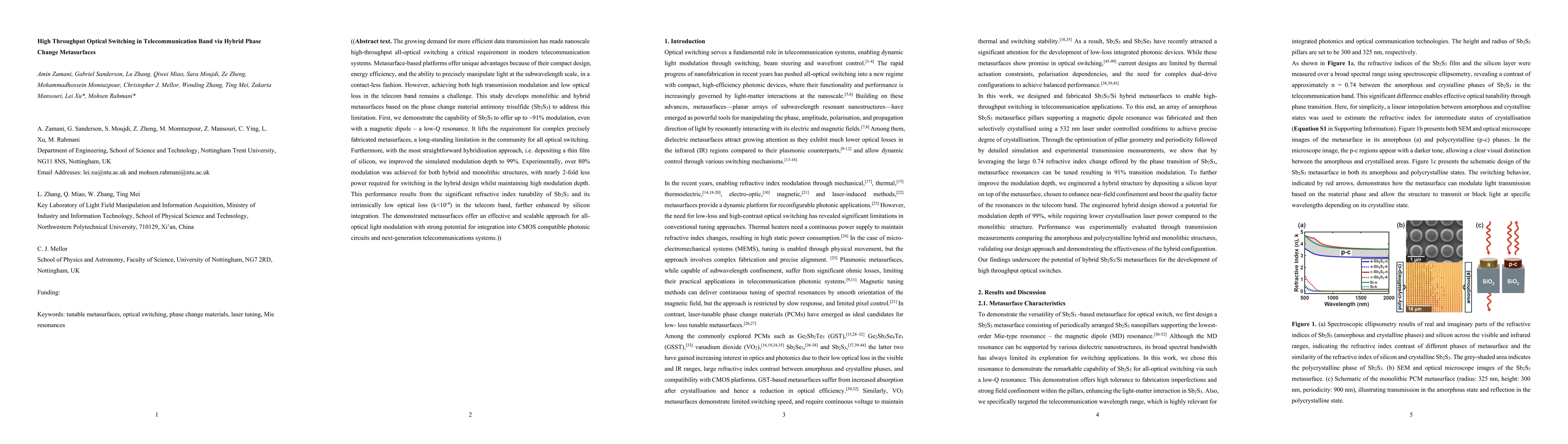
The growing demand for more efficient data transmission has made nanoscale
high-throughput all-optical switching a critical requirement in modern
telecommunication systems. Metasurface-based platforms offer unique advantages
because of their compact design, energy efficiency, and the ability to
precisely manipulate light at the subwavelength scale, in a contact-less
fashion. However, achieving both high transmission modulation and low optical
loss in the telecom band remains a challenge. This study develops monolithic
and hybrid metasurfaces based on the phase change material antimony trisulfide
(Sb$_2$S$_3$) to address this limitation. First, we demonstrate the capability
of Sb$_2$S$_3$ to offer up to ~91 percent modulation, even with a magnetic
dipole - a low-Q resonance. It lifts the requirement for complex precisely
fabricated metasurfaces, a long-standing limitation in the community for all
optical switching. Furthermore, with the most straightforward hybridisation
approach, i.e. depositing a thin film of silicon, we improved the simulated
modulation depth to 99 percent. Experimentally, over 80 percent modulation was
achieved for both hybrid and monolithic structures, with nearly 2-fold less
power required for switching in the hybrid design whilst maintaining high
modulation depth. This performance results from the significant refractive
index tunability of Sb$_2$S$_3$ and its intrinsically low optical loss (k <
10^{-4}) in the telecom band, further enhanced by silicon integration. The
demonstrated metasurfaces offer an effective and scalable approach for
all-optical light modulation with strong potential for integration into
CMOS-compatible photonic circuits and next-generation telecommunications
systems.
Discussion 0