High-throughput spin-bath characterization of spin-defects in semiconductors
Publication
Metrics
AI Quick Summary
This research introduces a high-throughput method using Bayesian inference to characterize spin-defects in semiconductors, like NV centers in diamond or divacancies in silicon carbide. The method rapidly determines atomic positions, hyperfine couplings, and nuclear spin locations, enabling efficient screening of spin-defects for quantum applications and guiding experimental design for dynamical decoupling experiments.
Paper Preview
Abstract
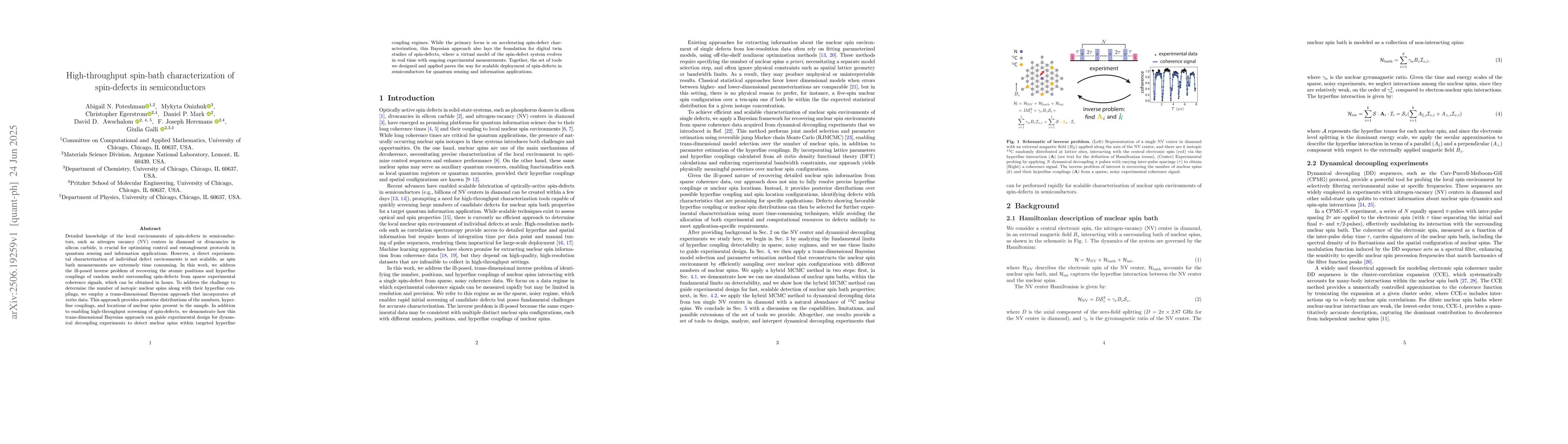
Detailed knowledge of the local environments of spin-defects in semiconductors, such as nitrogen vacancy (NV) centers in diamond or divacancies in silicon carbide, is crucial for optimizing control and entanglement protocols in quantum sensing and information applications. However, a direct experimental characterization of individual defect environments is not scalable, as spin bath measurements are extremely time consuming. In this work, we address the ill-posed inverse problem of recovering the atomic positions and hyperfine couplings of random nuclei surrounding spin-defects from sparse experimental coherence signals, which can be obtained in hours. To address the challenge to determine the number of isotopic nuclear spins along with their hyperfine couplings, we employ a trans-dimensional Bayesian approach that incorporates ab initio data. This approach provides posterior distributions of the numbers, hyperfine couplings, and locations of nuclear spins present in the sample. In addition to enabling high-throughput screening of spin-defects, we demonstrate how this trans-dimensional Bayesian approach can guide experimental design for dynamical decoupling experiments to detect nuclear spins within targeted hyperfine coupling regimes. While the primary focus is on accelerating spin-defect characterization, this Bayesian approach also lays the foundation for digital twin studies of spin-defects, where a virtual model of the spin-defect system evolves in real time with ongoing experimental measurements. Together, the set of tools we designed and applied paves the way for scalable deployment of spin-defects in semiconductors for quantum sensing and information applications.
AI Key Findings
Get AI-generated insights about this paper's methodology, results, significance, and more — seven facets brought into focus.
Impact
Paper Details
Authors
PDF Preview
Citation Network
Current paper (gray), citations (green), references (blue)
Display is limited for performance on very large graphs.
Discussion 0