Publication
Metrics
AI Quick Summary
This paper introduces a novel deterministic transfer system for two-dimensional materials that achieves high accuracy, reliability, and non-contaminating transfer, addressing the need for precise, multi-substrate, and contamination-free 2D material processing. The system demonstrates its effectiveness by fabricating optoelectronic devices, showcasing rapid prototyping without wet chemistry.
Paper Preview
Abstract
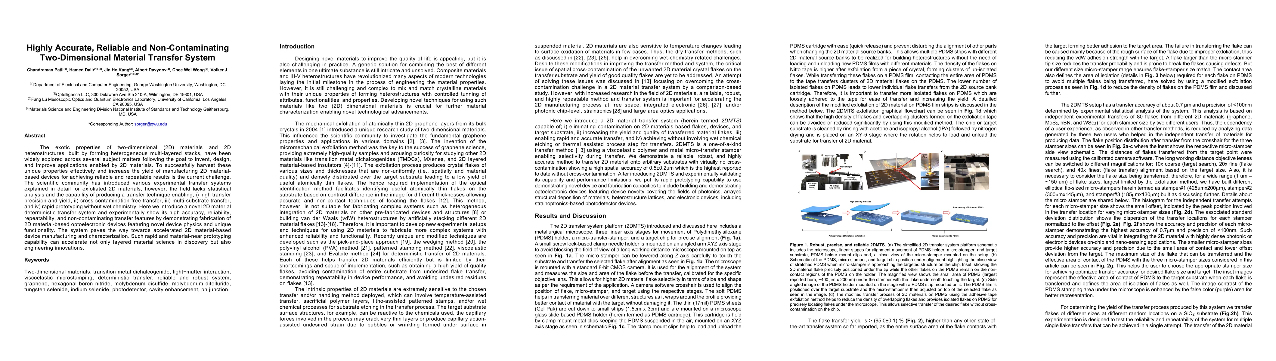
The exotic properties of two-dimensional (2D) materials and 2D heterostructures, built by forming heterogeneous multi-layered stacks, have been widely explored across a number of subject matters following the goal to invent, design, and improve applications enabled by 2D materials. To successfully harvest these unique properties effectively and increase the yield of manufacturing 2D material-based devices for achieving reliable and repeatable results is the current challenge. The scientific community has introduced various experimental transfer systems explained in detail for exfoliated 2D materials, however, the field lacks statistical analysis and the capability of producing a transfer technique enabling; i) high transfer precision and yield, ii) cross-contamination free transfer, iii) multi-substrate transfer, and iv) rapid prototyping without wet chemistry. Here we introduce a novel 2D material deterministic transfer system and experimentally show its high accuracy, reliability, repeatability, and non-contaminating transfer features by demonstrating fabrication of 2D material-based optoelectronic devices featuring novel device physics and unique functionality. Such rapid and material-near prototyping capability can accelerate not only layered material science in discovery but also engineering innovations.
AI Key Findings
Get AI-generated insights about this paper's methodology, results, significance, and more — seven facets brought into focus.
Impact
Paper Details
Authors
PDF Preview
Key Terms
Citation Network
Current paper (gray), citations (green), references (blue)
Display is limited for performance on very large graphs.
Discussion 0