01
MethodologyHow they did it
The PdCoO2 thin films were grown using a combination of pulsed laser deposition and molecular beam epitaxy.
This paper reports the synthesis of highly conductive PdCoO2 ultrathin films via pulsed laser deposition, demonstrating exceptional electrical conductivity and optical transparency, making them promising candidates for transparent electrode applications.
This paper reports the synthesis of highly conductive PdCoO2 ultrathin films via pulsed laser deposition, demonstrating exceptional electrical conductivity and optical transparency, making them promising candidates for transparent electrode applications.
The PdCoO2 thin films were grown using a combination of pulsed laser deposition and molecular beam epitaxy. More in Methodology →
The 2θ-ω XRD patterns showed a clear epitaxial relationship between the PdCoO2 film and the Al2O3 substrate. — The AFM topographic image revealed two triangular shapes corresponding to two domains in the PdCoO2 film. More in Key Results →
This research demonstrates a new epitaxial relationship between PdCoO2 and Al2O3, which is crucial for understanding the electronic properties of PdCoO2. More in Significance →
The XRD patterns did not provide clear information on the in-plane lattice configurations of the Pd layer and CoO2 layers. — The AFM image only revealed two domains in the PdCoO2 film, which may not be representative of the entire film. More in Limitations →
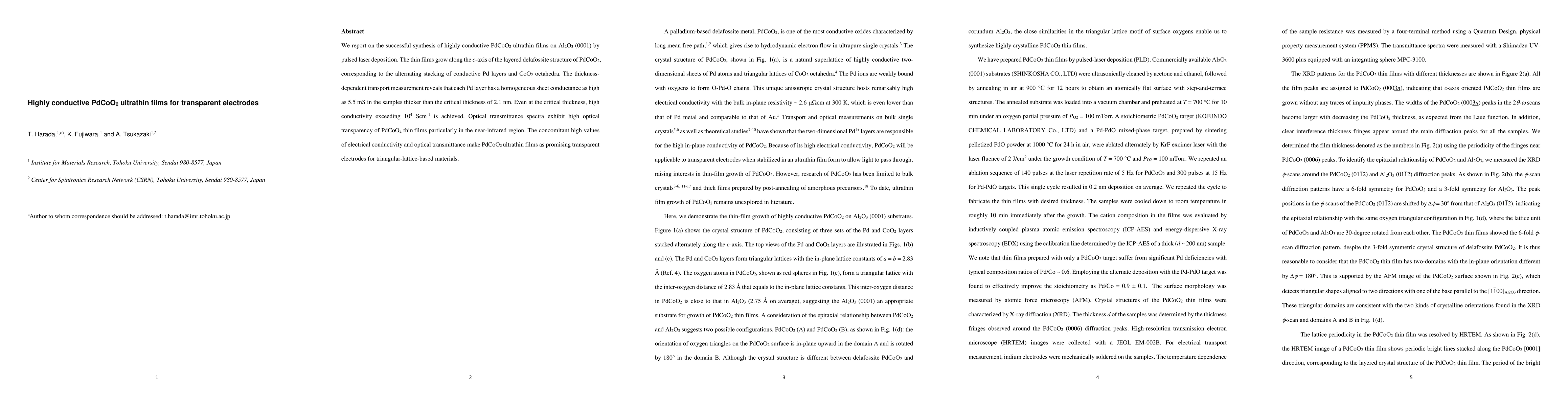
We report on the successful synthesis of highly conductive PdCoO2 ultrathin films on Al2O3 (0001) by pulsed laser deposition. The thin films grow along the c-axis of the layered delafossite structure of PdCoO2, corresponding to the alternating stacking of conductive Pd layers and CoO2 octahedra. The thickness-dependent transport measurement reveals that each Pd layer has a homogeneous sheet conductance as high as 5.5 mS in the samples thicker than the critical thickness of 2.1 nm. Even at the critical thickness, high conductivity exceeding 104 Scm-1 is achieved. Optical transmittance spectra exhibit high optical transparency of PdCoO2 thin films particularly in the near-infrared region. The concomitant high values of electrical conductivity and optical transmittance make PdCoO2 ultrathin films as promising transparent electrodes for triangular-lattice-based materials.
Seven facets of this paper, analysed and brought into focus by AI.
This research demonstrates a new epitaxial relationship between PdCoO2 and Al2O3, which is crucial for understanding the electronic properties of PdCoO2.
The PdCoO2 thin films were grown using a combination of pulsed laser deposition and molecular beam epitaxy.
This research demonstrates a new epitaxial relationship between PdCoO2 and Al2O3, which is crucial for understanding the electronic properties of PdCoO2.
This work presents a new epitaxial relationship between PdCoO2 and Al2O3, which is essential for understanding the electronic properties of PdCoO2.
The epitaxial relationship presented in this work is novel because it provides new insights into the crystal structure of PdCoO2 on Al2O3.
Current paper (gray), citations (green), references (blue)
Display is limited for performance on very large graphs.
Discussion 0