This paper introduces two novel fabrication techniques—etch-and-oversputter (EnS) and deposit-and-oversputter (DnS)—for creating hybrid confinement in III-V semiconductor microcavities, achieving deep, controllable potentials and high-quality optical band structures. The methods enable precise control over lattice couplings and facilitate the creation of complex photonic structures for quantum simulation and advanced photonic applications.
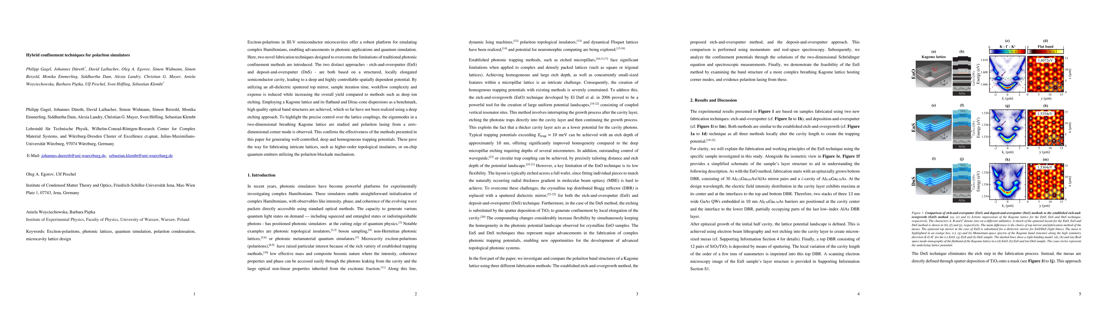
Exciton-polaritons in III-V semiconductor microcavities offer a robust platform for emulating complex Hamiltonians, enabling advancements in photonic applications and quantum simulation. Here, two novel fabrication techniques designed to overcome the limitations of traditional photonic confinement methods are introduced. The two distinct approaches - etch-and-oversputter (EnS) and deposit-and-oversputter (DnS) - are both based on a structured, locally elongated semiconductor cavity, leading to a deep and highly controllable spatially dependent potential. By utilizing an all-dielectric sputtered top mirror, sample iteration time, workflow complexity and expense is reduced while increasing the overall yield compared to methods such as deep ion etching. Employing a Kagome lattice and its flatband and Dirac-cone dispersions as a benchmark, high quality optical band structures are achieved, which so far have not been realized using a deep etching approach. To highlight the precise control over the lattice couplings, the eigenmodes in a two-dimensional breathing Kagome lattice are studied and polariton lasing from a zerodimensional corner mode is observed. This confirms the effectiveness of the methods presented in this paper for generating well-controlled, deep and homogeneous trapping potentials. These pave the way for fabricating intricate lattices, such as higher-order topological insulators, or on-chip quantum emitters utilizing the polariton blockade mechanism.
Generated Jun 10, 2025
The research introduces two novel fabrication techniques, etch-and-oversputter (EnS) and deposit-and-oversputter (DnS), for creating uniform potential landscapes in microcavities using all-dielectric mirrors. These methods simplify fabrication and reduce iteration time, enabling the creation of complex potential landscapes with high precision.
This work paves the way for emulating and studying various complex Hamiltonians, including higher-order topological insulators, and represents a significant step toward investigating the polariton blockade mechanism in resonators with small mode volume.
The paper presents innovative fabrication techniques that simplify the creation of complex potential landscapes in microcavities, leading to improved yield and reduced fabrication time.
The hybrid confinement techniques (EnS and DnS) offer a novel approach to microcavity fabrication, overcoming limitations of traditional photonic confinement methods and enabling precise control over spatially dependent potentials.
No key terms available for this paper.
Current paper (gray), citations (green), references (blue)
A. Kudlis, I. A. Shelykh, D. Novokreschenov
No citations found for this paper.
Comments (0)