Publication
Metrics
AI Quick Summary
This paper demonstrates a hybrid integration technique for solid-state quantum emitters, specifically InAs/InP quantum dots, onto silicon photonic chips using pick-and-place methods with nanoscale precision. An adiabatic tapering approach is used to efficiently transfer quantum dot emissions into the silicon waveguide, enabling scalable and complex quantum photonic systems.
Paper Preview
Abstract
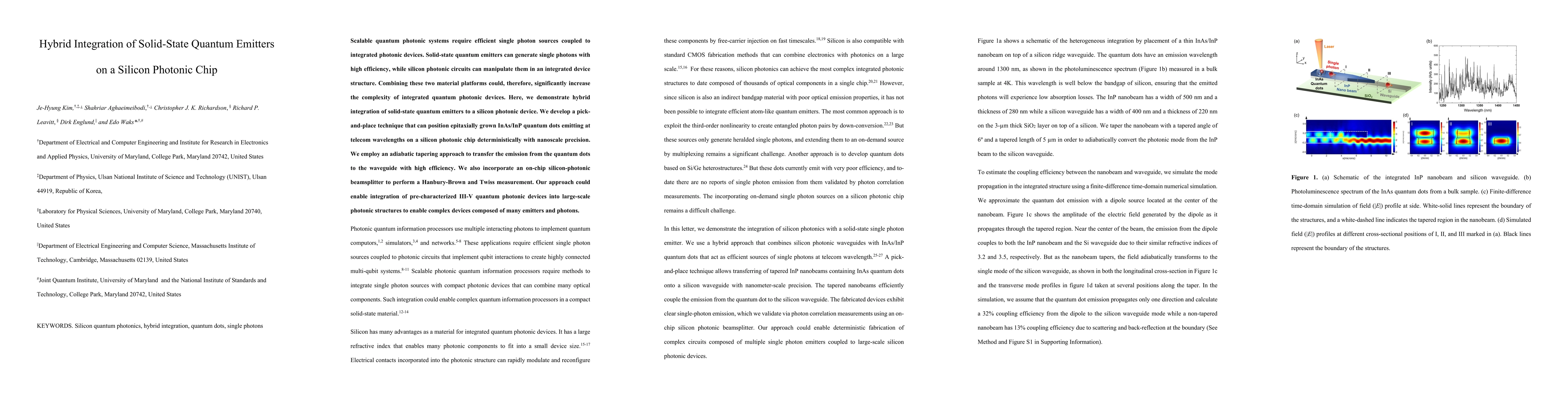
Scalable quantum photonic systems require efficient single photon sources coupled to integrated photonic devices. Solid-state quantum emitters can generate single photons with high efficiency, while silicon photonic circuits can manipulate them in an integrated device structure. Combining these two material platforms could, therefore, significantly increase the complexity of integrated quantum photonic devices. Here, we demonstrate hybrid integration of solid-state quantum emitters to a silicon photonic device. We develop a pick-and-place technique that can position epitaxially grown InAs/InP quantum dots emitting at telecom wavelengths on a silicon photonic chip deterministically with nanoscale precision. We employ an adiabatic tapering approach to transfer the emission from the quantum dots to the waveguide with high efficiency. We also incorporate an on-chip silicon-photonic beamsplitter to perform a Hanbury-Brown and Twiss measurement. Our approach could enable integration of pre-characterized III-V quantum photonic devices into large-scale photonic structures to enable complex devices composed of many emitters and photons.
AI Key Findings
Get AI-generated insights about this paper's methodology, results, significance, and more — seven facets brought into focus.
Impact
Paper Details
PDF Preview
Key Terms
Citation Network
Current paper (gray), citations (green), references (blue)
Display is limited for performance on very large graphs.
Discussion 0