Summary
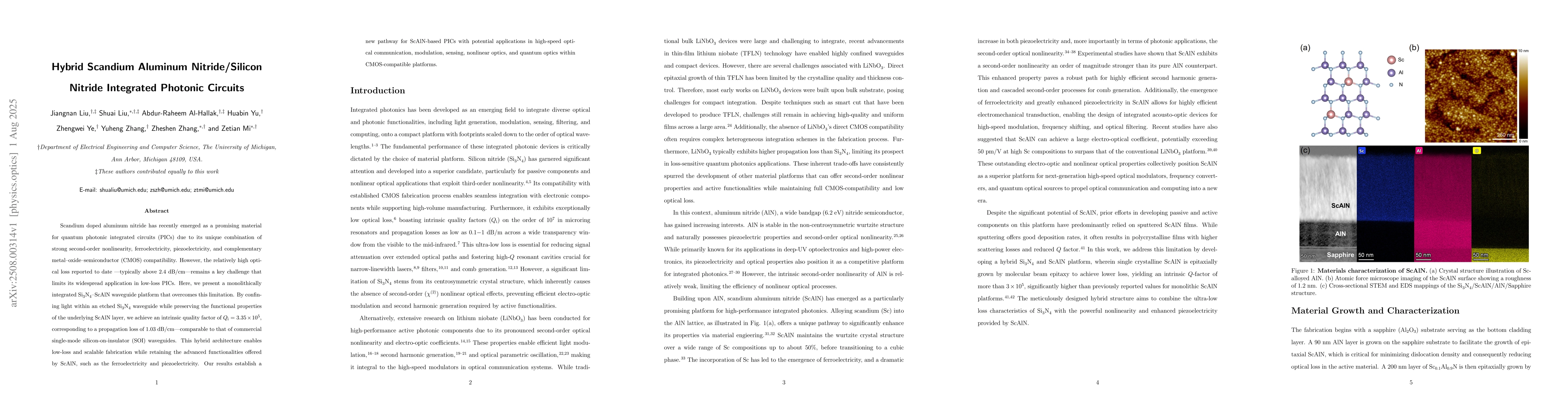
Scandium-doped aluminum nitride has recently emerged as a promising material for quantum photonic integrated circuits (PICs) due to its unique combination of strong second-order nonlinearity, ferroelectricity, piezoelectricity, and complementary metal-oxide-semiconductor (CMOS) compatibility. However, the relatively high optical loss reported to date-typically above 2.4 dB/cm-remains a key challenge that limits its widespread application in low-loss PICs. Here, we present a monolithically integrated $\mathrm{Si}_3\mathrm{N}_4$-ScAlN waveguide platform that overcomes this limitation. By confining light within an etched $\mathrm{Si}_3\mathrm{N}_4$ waveguide while preserving the functional properties of the underlying ScAlN layer, we achieve an intrinsic quality factor of $Q_{\mathrm{i}} = 3.35 \times 10^5$, corresponding to a propagation loss of 1.03 dB/cm-comparable to that of commercial single-mode silicon-on-insulator (SOI) waveguides. This hybrid architecture enables low-loss and scalable fabrication while retaining the advanced functionalities offered by ScAlN, such as ferroelectricity and piezoelectricity. Our results establish a new pathway for ScAlN-based PICs with potential applications in high-speed optical communication, modulation, sensing, nonlinear optics, and quantum optics within CMOS-compatible platforms.
AI Key Findings
Generated Sep 02, 2025
Methodology
The research employs a monolithic integration approach of Si3N4 and ScAlN layers using a recently developed amorphous silicon (a-Si) hardmask dry etching technique, enabling high-selectivity and smooth Si3N4 waveguides. The fabrication process includes MBE-grown ScAlN film on AlN-on-Al2O3 wafer, LPCVD deposition of 500 nm Si3N4, EBL, thermal reflow, RIE, XeF2 vapor etching, and PECVD deposition of SiO2 top cladding.
Key Results
- Achieved an intrinsic quality factor (Qi) of 3.35 × 10^5 for Si3N4-ScAlN microring resonators, corresponding to a propagation loss of 1.03 dB/cm.
- Demonstrated low-loss and scalable fabrication of hybrid Si3N4-ScAlN photonic circuits, retaining ScAlN's advanced functionalities such as ferroelectricity and piezoelectricity.
- Implemented Euler racetrack design to further reduce optical loss in microring resonators, achieving a maximum Qi of 3.35 × 10^5 with a propagation loss of 1.03 dB/cm.
Significance
This research presents a CMOS-compatible platform with competitive low-loss characteristics suitable for next-generation integrated photonics, featuring additional functionalities like high χ(2) nonlinearity, ferroelectricity, and piezoelectricity.
Technical Contribution
The paper presents a novel monolithically integrated Si3N4-ScAlN photonic platform with an intrinsic quality factor of Qi = 3.35 × 10^5, corresponding to a propagation loss of 1.03 dB/cm, enabling low-loss and scalable fabrication while retaining ScAlN's advanced functionalities.
Novelty
This work is novel as it overcomes the high optical loss limitation of ScAlN by confining light within an etched Si3N4 waveguide, preserving ScAlN's functional properties and offering a CMOS-compatible platform for high-speed optical communication, modulation, sensing, nonlinear optics, and quantum optics.
Limitations
- The study did not explore the long-term stability and reliability of the hybrid Si3N4-ScAlN photonic circuits.
- The research focused on microring resonators, and further studies are needed to validate the performance in other photonic components.
Future Work
- Investigate the long-term stability and reliability of the hybrid Si3N4-ScAlN photonic circuits.
- Explore the applicability of this platform in various photonic components beyond microring resonators.
Paper Details
PDF Preview
Citation Network
Current paper (gray), citations (green), references (blue)
Display is limited for performance on very large graphs.
Similar Papers
Found 4 papersSilicon-integrated scandium-doped aluminum nitride electro-optic modulator
Tao Wu, Tianqi Xu, Yang Qiu et al.
Aluminum nitride integration on silicon nitride photonic circuits: a new hybrid approach towards on-chip nonlinear optics
Rudolf Gross, Manuel Müller, Matthias Althammer et al.
No citations found for this paper.
Comments (0)