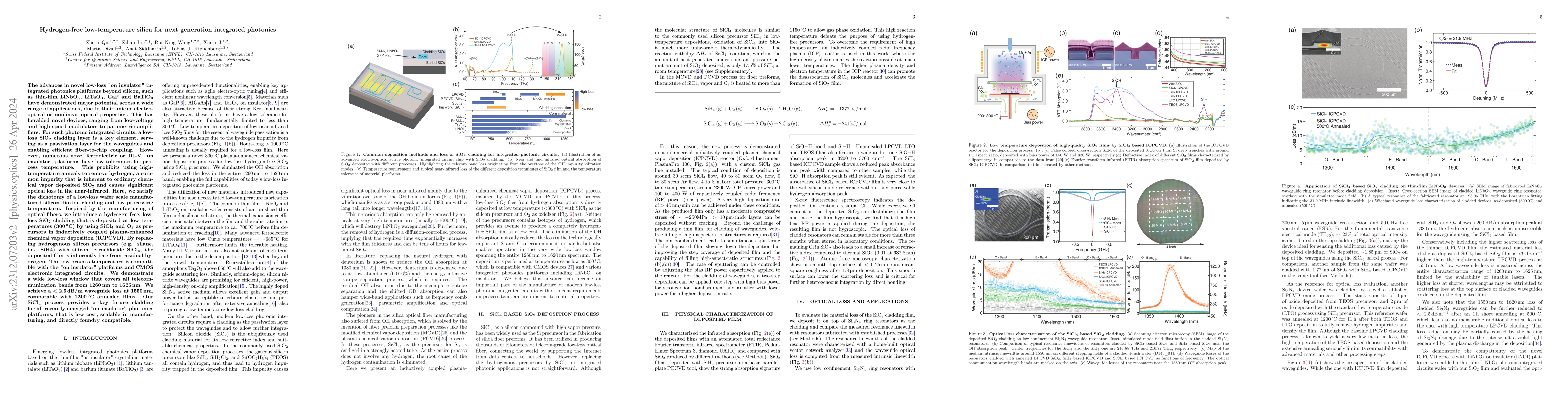
The advances in novel low-loss "on insulator" integrated photonics platforms
beyond silicon, such as thin-film LiNbO3, LiTaO3, GaP and BaTiO3 have
demonstrated major potential across a wide range of applications, due to their
unique electro-optical or nonlinear optical properties. This has heralded novel
devices, ranging from low-voltage and high-speed modulators to parametric
amplifiers. For such photonic integrated circuits, a low-loss SiO2 cladding
layer is a key element, serving as a passivation layer for the waveguides and
enabling efficient fiber-to-chip coupling. However, numerous novel
ferroelectric or III-V "on insulator" platforms have low tolerances for process
temperature. This prohibits using high-temperature anneals to remove hydrogen,
a common impurity that is inherent to ordinary chemical vapor deposited SiO2
and causes significant optical loss in the near infrared. Here, we satisfy the
dichotomy of a low-loss wafer scale manufactured SiO2 cladding and low
processing temperature. Inspired by the manufacturing of optical fibers, we
introduce a hydrogen-free, low-loss SiO2 cladding that is deposited at low
temperatures (300 degrees Celsius) by using SiCl4 and O2 as precursors in
inductively coupled plasma-enhanced chemical vapor deposition (ICPCVD). By
replacing hydrogenous silicon precursors (e.g. SiH4) with SiCl4, the deposited
film is inherently free from residual hydrogen. The process temperature is
compatible with the "on insulator" platforms and CMOS electronic integrated
circuits. We demonstrate a wide low-loss window that covers all
telecommunication bands from 1260 nm to 1625 nm. We achieve a < 2.5 dB/m
waveguide loss at 1550 nm, comparable with 1200 degree Celsius annealed films.
Our SiCl4 process provides a key future cladding for all recently emerged
"on-insulator" photonics platforms, that is low cost, scalable in
manufacturing, and directly foundry compatible.
Discussion 0