Publication
Metrics
AI Quick Summary
This paper proposes a novel detection method for atomically thin crystals using diffusively reflected light on optically inhomogeneous substrates, which enhances optical contrast and polarization properties. This approach offers improved sensitivity and the ability to detect layers on non-traditional substrates, providing an alternative to conventional Fabry-Perot interference-based detection.
Paper Preview
Abstract
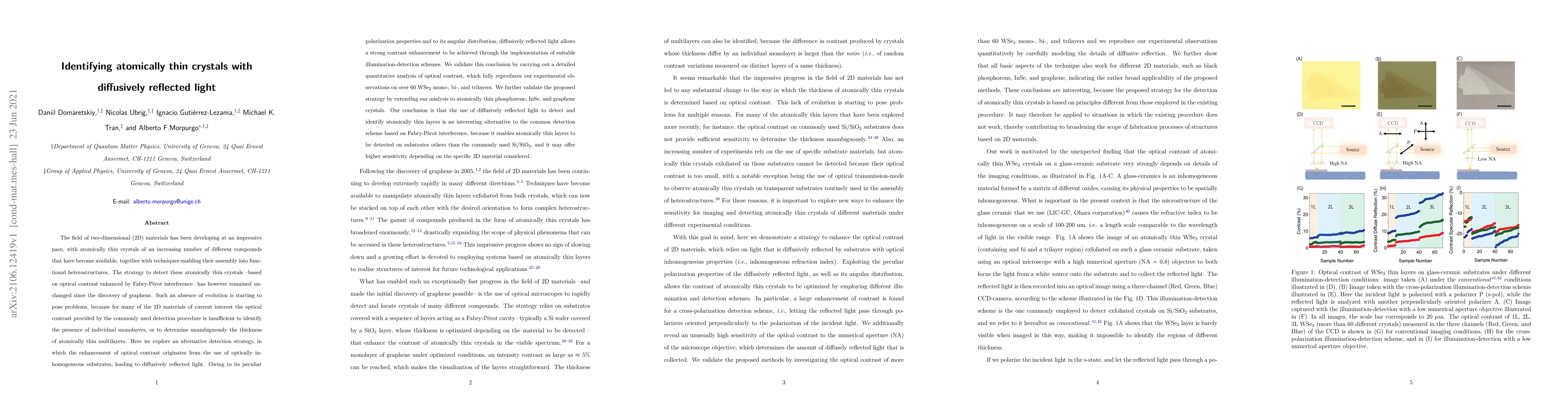
The field of two-dimensional materials has been developing at an impressive pace, with atomically thin crystals of an increasing number of different compounds that have become available, together with techniques enabling their assembly into functional heterostructures. The strategy to detect these atomically thin crystals has however remained unchanged since the discovery of graphene. Such an absence of evolution is starting to pose problems because for many of the 2D materials of current interest the optical contrast provided by the commonly used detection procedure is insufficient to identify the presence of individual monolayers or to determine unambiguously the thickness of atomically thin multilayers. Here we explore an alternative detection strategy, in which the enhancement of optical contrast originates from the use of optically inhomogeneous substrates, leading to diffusively reflected light. Owing to its peculiar polarization properties and to its angular distribution, diffusively reflected light allows a strong contrast enhancement to be achieved through the implementation of suitable illumination-detection schemes. We validate this conclusion by carrying out a detailed quantitative analysis of optical contrast, which fully reproduces our experimental observations on over 60 WSe$_2$ mono-, bi-, and trilayers. We further validate the proposed strategy by extending our analysis to atomically thin phosphorene, InSe, and graphene crystals. Our conclusion is that the use of diffusively reflected light to detect and identify atomically thin layers is an interesting alternative to the common detection scheme based on Fabry-Perot interference, because it enables atomically thin layers to be detected on substrates others than the commonly used Si/SiO$_2$, and it may offer higher sensitivity depending on the specific 2D material considered.
AI Key Findings
Get AI-generated insights about this paper's methodology, results, significance, and more — seven facets brought into focus.
Impact
Paper Details
Authors
PDF Preview
Key Terms
Citation Network
Current paper (gray), citations (green), references (blue)
Display is limited for performance on very large graphs.
Discussion 0