ArxivLens
ArXiv physics.app-ph

III-V-on-silicon triple-junction based on the heterojunction bipolar transistor solar cell concept

A. Marti, E. Antolin, M. H. Zehender, P. G. Linares, S. A. Svatek

2105.03222 2020 47th IEEE Photovoltaic Specialists Conference (PVSC) DOI: 10.1109/PVSC45281.2020.9300681 Published May 10, 2021
View PDF

Publication

Published: May 10, 2021
Categories: physics.app-ph

Metrics

Source: ArXiv

AI Quick Summary

This research proposes a novel III-V-on-silicon triple-junction solar cell using a heterojunction bipolar transistor solar cell (HBTSC) stacked on a silicon cell. The new structure achieves a theoretical efficiency limit comparable to conventional triple junctions but with a wider operational band-gap range, particularly promising for GaInP/GaAs materials.

Quick Answers

What is "III-V-on-silicon triple-junction based on the heterojunction bipolar transistor solar cell concept" about?

This research proposes a novel III-V-on-silicon triple-junction solar cell using a heterojunction bipolar transistor solar cell (HBTSC) stacked on a silicon cell. The new structure achieves a theoretical efficiency limit comparable to conventional triple junctions but with a wider operational band-gap range, particularly promising for GaInP/GaAs materials.

What methodology did the authors use?

The research proposes a new III-V-on-silicon triple-junction solar cell structure using a heterojunction bipolar transistor solar cell (HBTSC) stacked on top of a Si solar cell, with detailed balance efficiency limit calculations performed under one-sun illumination. More in Methodology →

What are the key results?

The absolute efficiency limit of a III-V-HBTSC-on-Si device is the same as for a conventional current-matched III-V-on-Si triple-junction (47% with black-body spectrum, 49% with AM1.5G spectrum). — The range of band-gap energies for which the efficiency limit is above 40% is much wider in the III-V-HBTSC-on-Si stack case. More in Key Results →

Why is this work significant?

This research presents a promising device, GaInP/GaAs-HBTSC-on-Si, for high-efficiency one-sun operation, which could be cost-effective with low-cost III-V material growth technologies. More in Significance →

What are the main limitations?

The study assumes ideal conditions and does not account for practical manufacturing challenges and losses. — The efficiency limits are based on detailed balance calculations and may not fully represent real-world performance. More in Limitations →

Paper Preview

Abstract

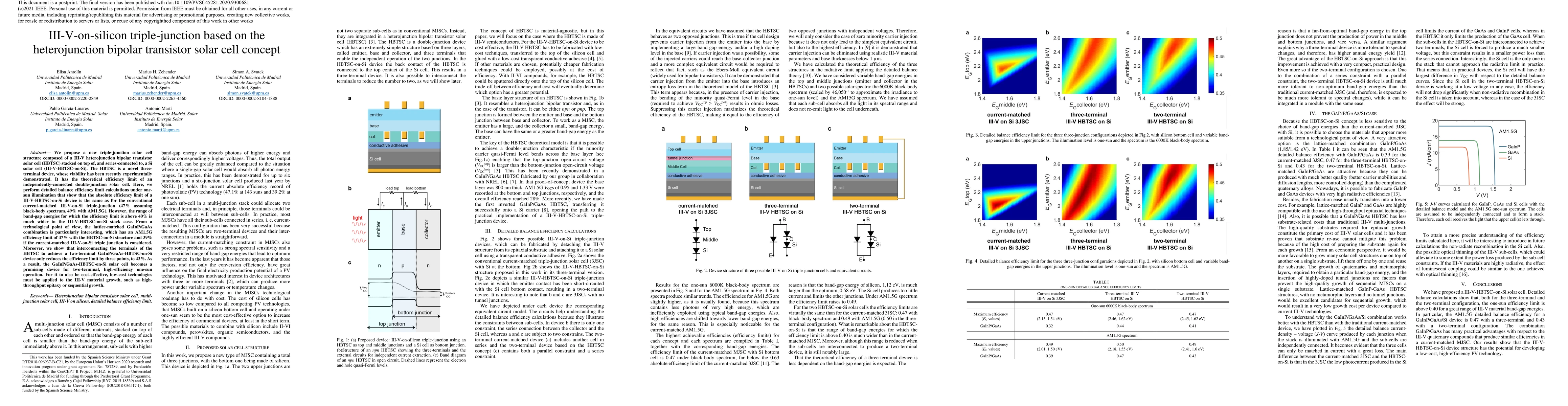
We propose a new triple-junction solar cell structure composed of a III-V heterojunction bipolar transistor solar cell (HBTSC) stacked on top of, and series-connected to, a Si solar cell (III-V-HBTSC-on-Si). The HBTSC is a novel three-terminal device, whose viability has been recently experimentally demonstrated. It has the theoretical efficiency limit of an independently-connected double-junction solar cell. Here, we perform detailed balance efficiency limit calculations under one-sun illumination that show that the absolute efficiency limit of a III-V-HBTSC-on-Si device is the same as for the conventional current-matched III-V-on-Si triple-junction (47% assuming black-body spectrum, 49% with AM1.5G). However, the range of band-gap energies for which the efficiency limit is above 40% is much wider in the III-V-HBTSC-on-Si stack case. From a technological point of view, the lattice-matched GaInP/GaAs combination is particularly interesting, which has an AM1.5G efficiency limit of 47% with the HBTSC-on-Si structure and 39% if the current-matched III-V-on-Si triple junction is considered. Moreover, we show that interconnecting the terminals of the HBTSC to achieve a two-terminal GaInP/GaAs-HBTSC-on-Si device only reduces the efficiency limit by three points, to 43%. As a result, the GaInP/GaAs-HBTSC-on-Si solar cell becomes a promising device for two-terminal, high-efficiency one-sun operation. For it to also be cost-effective, low-cost technologies must be applied to the III-V material growth, such as high-throughput epitaxy or sequential growth.

Key Findings, in focus

Seven facets of this paper, analysed and brought into focus by AI.

AI-generated · verify against source Generated Sep 02, 2025
In focus · one-line synthesis

This research presents a promising device, GaInP/GaAs-HBTSC-on-Si, for high-efficiency one-sun operation, which could be cost-effective with low-cost III-V material growth technologies.

01
MethodologyHow they did it

The research proposes a new III-V-on-silicon triple-junction solar cell structure using a heterojunction bipolar transistor solar cell (HBTSC) stacked on top of a Si solar cell, with detailed balance efficiency limit calculations performed under one-sun illumination.

02
ResultsWhat they found
  • The absolute efficiency limit of a III-V-HBTSC-on-Si device is the same as for a conventional current-matched III-V-on-Si triple-junction (47% with black-body spectrum, 49% with AM1.5G spectrum).
  • The range of band-gap energies for which the efficiency limit is above 40% is much wider in the III-V-HBTSC-on-Si stack case.
  • For a lattice-matched GaInP/GaAs combination, the AM1.5G efficiency limit is 47% with HBTSC-on-Si, compared to 39% for a current-matched III-V-on-Si triple junction.
  • Interconnecting the HBTSC terminals to form a two-terminal GaInP/GaAs-HBTSC-on-Si device reduces the efficiency limit by only three points, to 43%.
03
SignificanceWhy it matters

This research presents a promising device, GaInP/GaAs-HBTSC-on-Si, for high-efficiency one-sun operation, which could be cost-effective with low-cost III-V material growth technologies.

04
Technical ContributionsWhat's new technically

The paper introduces a novel III-V-HBTSC-on-Si solar cell structure and performs detailed balance efficiency limit calculations, demonstrating its potential for high-efficiency one-sun operation.

05
NoveltyWhat sets it apart

The proposed III-V-HBTSC-on-Si structure offers a new approach to high-efficiency solar cells, with a wider range of band-gap energies for achieving high efficiency compared to conventional current-matched triple-junctions.

06
LimitationsWhat to be cautious about
  • The study assumes ideal conditions and does not account for practical manufacturing challenges and losses.
  • The efficiency limits are based on detailed balance calculations and may not fully represent real-world performance.
07
Future WorkWhere it goes next
  • Further research should focus on implementing low-cost III-V material growth techniques, such as high-throughput epitaxy or sequential growth.
  • Experimental validation of the proposed device's performance is necessary to confirm the theoretical efficiency limits.

Impact

15
References

Paper Details

Paper ID: 2105.03222
Journal: 2020 47th IEEE Photovoltaic Specialists Conference (PVSC)
License: http://creativecommons.org/licenses/by-nc-nd/4.0/
Categories:
physics.app-ph

How to Cite This Paper

Reference manager: RIS EndNote

Key Terms

si (0.316)
si (0.300)
iii (0.262)
iii (0.246)
junction (0.244)
junction (0.235)
terminal (0.227)
cell (0.225)

Citation Network

Current paper (gray), citations (green), references (blue)

Display is limited for performance on very large graphs.

Current Paper
Citations
References
Click to view


Discussion 0

This website uses cookies to ensure you get the best experience. Learn more