Imaging carrier transport properties in halide perovskites using time-resolved optical microscopy
Publication
Metrics
Paper Preview
Abstract
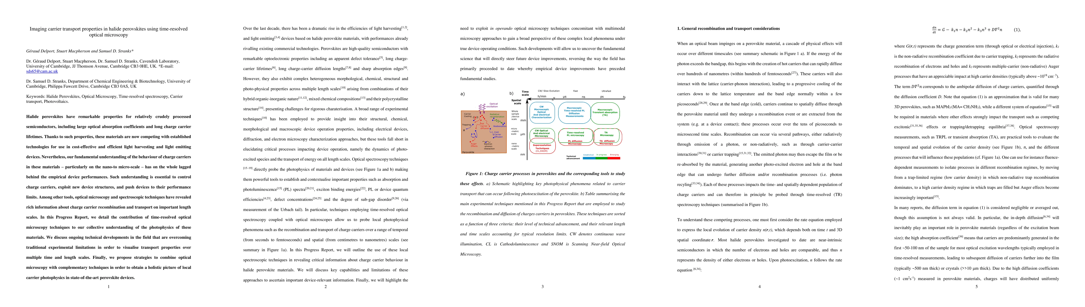
Halide perovskites have remarkable properties for relatively crudely processed semiconductors, including large optical absorption coefficients and long charge carrier lifetimes. Thanks to such properties, these materials are now competing with established technologies for use in cost-effective and efficient light harvesting and light emitting devices. Nevertheless, our fundamental understanding of the behaviour of charge carriers in these materials particularly on the nano to micro scale has on the whole lagged behind the empirical device performances. Such understanding is essential to control charge carriers, exploit new device structures, and push devices to their performance limits. Among other tools, optical microscopy and spectroscopic techniques have revealed rich information about charge carrier recombination and transport on important length scales. In this Progress Report, we detail the contribution of time-resolved optical microscopy techniques to our collective understanding of the photophysics of these materials. We discuss ongoing technical developments in the field that are overcoming traditional experimental limitations in order to visualise transport properties over multiple time and length scales. Finally, we propose strategies to combine optical microscopy with complementary techniques in order to obtain a holistic picture of local carrier photophysics in state of the art perovskite devices.
AI Key Findings
Get AI-generated insights about this paper's methodology, results, significance, and more — seven facets brought into focus.
Impact
Paper Details
Authors
PDF Preview
Key Terms
Citation Network
Current paper (gray), citations (green), references (blue)
Display is limited for performance on very large graphs.
Discussion 0