Improving Electric Contacts to Two-Dimensional Semiconductors
Publication
Metrics
AI Quick Summary
Researchers found that contact resistance to two-dimensional semiconductors like MoS2 is 100 times larger than expected, highlighting the need for efficient interfaces to achieve low resistance for scaled devices.
Paper Preview
Abstract
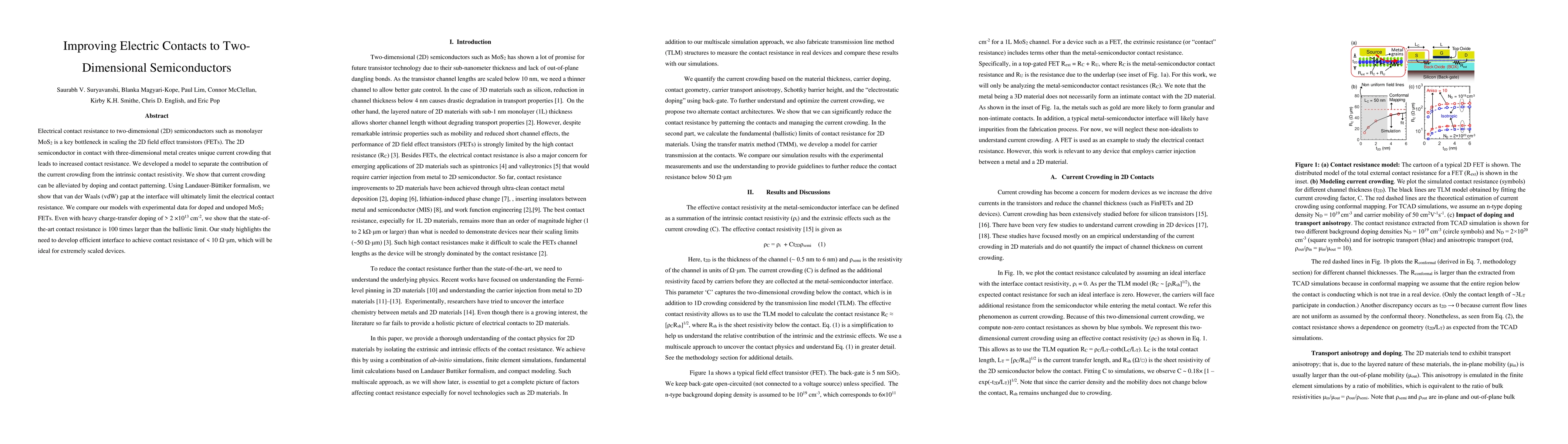
Electrical contact resistance to two-dimensional (2D) semiconductors such as monolayer MoS_{2} is a key bottleneck in scaling the 2D field effect transistors (FETs). The 2D semiconductor in contact with three-dimensional metal creates unique current crowding that leads to increased contact resistance. We developed a model to separate the contribution of the current crowding from the intrinsic contact resistivity. We show that current crowding can be alleviated by doping and contact patterning. Using Landauer-B\"uttiker formalism, we show that van der Waals (vdW) gap at the interface will ultimately limit the electrical contact resistance. We compare our models with experimental data for doped and undoped MoS_{2} FETs. Even with heavy charge-transfer doping of > 2x10^{13} cm^{-2}, we show that the state-of-the-art contact resistance is 100 times larger than the ballistic limit. Our study highlights the need to develop efficient interface to achieve contact resistance of < 10 {\Omega}.{\mu}m, which will be ideal for extremely scaled devices.
AI Key Findings
Get AI-generated insights about this paper's methodology, results, significance, and more — seven facets brought into focus.
Impact
Paper Details
Authors
PDF Preview
Key Terms
Citation Network
Current paper (gray), citations (green), references (blue)
Display is limited for performance on very large graphs.
Discussion 0