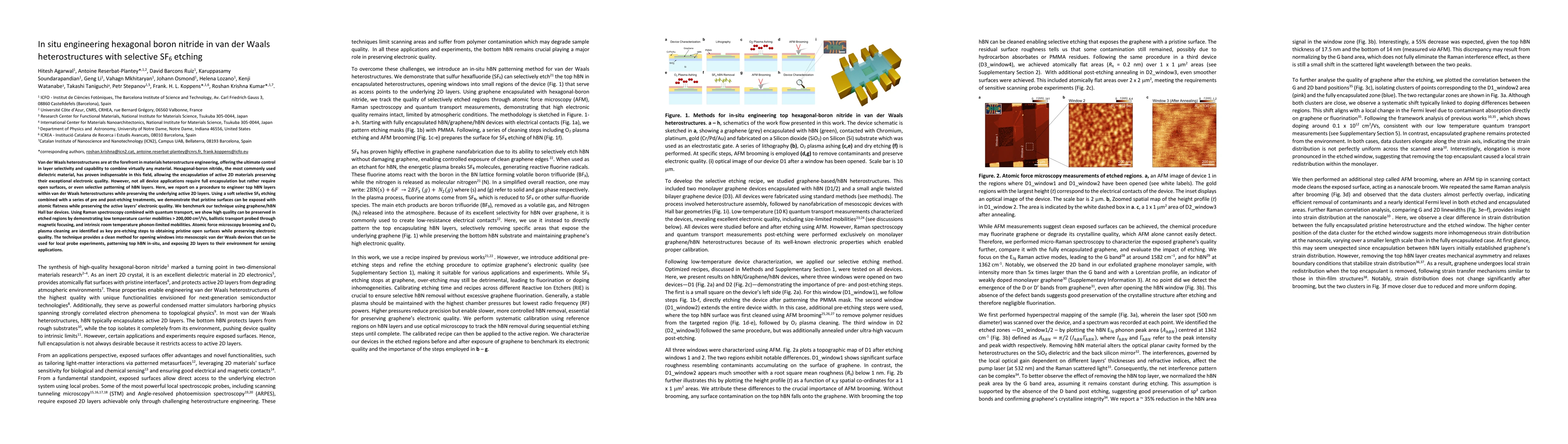
Van der Waals heterostructures are at the forefront in materials
heterostructure engineering, offering the ultimate control in layer selectivity
and capability to combine virtually any material. Hexagonal boron nitride
(hBN), the most commonly used dielectric material, has proven indispensable in
this field, allowing the encapsulation of active 2D materials preserving their
exceptional electronic quality. However, not all device applications require
full encapsulation but rather require open surfaces, or even selective
patterning of hBN layers. Here, we report on a procedure to engineer top hBN
layers within van der Waals heterostructures while preserving the underlying
active 2D layers. Using a soft selective SF6 etching combined with a series of
pre and post-etching treatments, we demonstrate that pristine surfaces can be
exposed with atomic flatness while preserving the active layers electronic
quality. We benchmark our technique using graphene encapsulated with hBN Hall
bar devices. Using Raman spectroscopy combined with quantum transport, we show
high quality can be preserved in etched regions by demonstrating low
temperature carrier mobilities of 200,000 cm2Vs-1, ballistic transport probed
through magnetic focusing, and intrinsic room temperature phonon-limited
mobilities. Atomic force microscopy brooming and O2 plasma cleaning are
identified as key pre-etching steps to obtaining pristine open surfaces while
preserving electronic quality. The technique provides a clean method for
opening windows into mesoscopic van der Waals devices that can be used for
local probe experiments, patterning top hBN in situ, and exposing 2D layers to
their environment for sensing applications.
Discussion 0