In-situ Patterned Damage-Free Etching of 3-Dimensional Structures in \b{eta}-Ga2O3 using Triethylgallium
Publication
Metrics
AI Quick Summary
This paper reports on the anisotropic etching of β-Ga2O3 using triethylgallium in a MOCVD chamber, revealing high anisotropy in sidewall roughness and etch rate due to its monoclinic structure. The method enables the creation of deep, sub-micron fins with smooth sidewalls and high aspect ratios without damaging the material, confirmed by undamaged Schottky diodes.
Paper Preview
Abstract
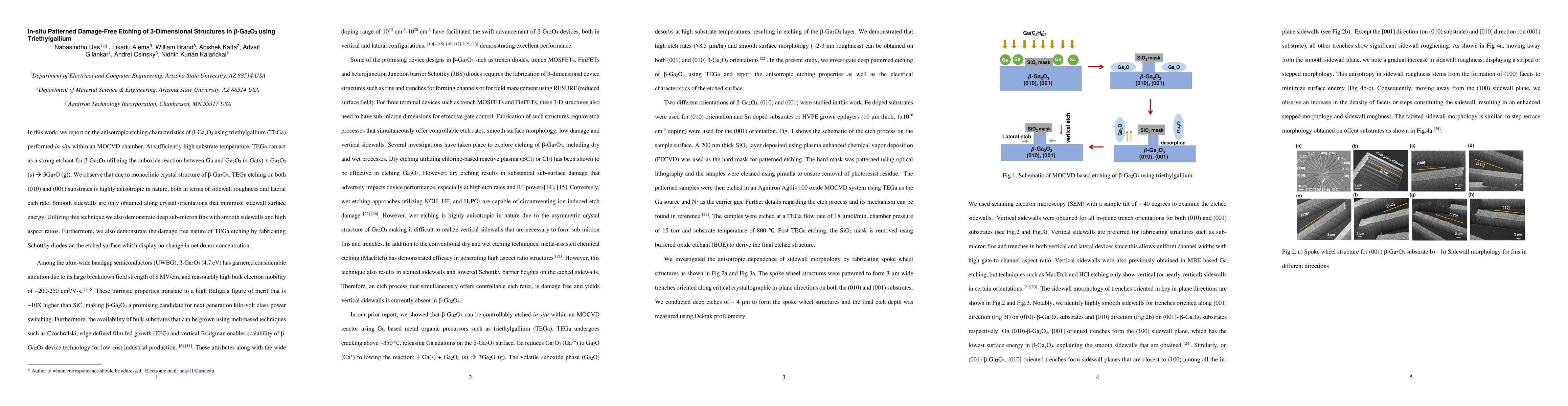
In this work, we report on the anisotropic etching characteristics of \b{eta}-Ga2O3 using triethylgallium (TEGa) performed in-situ within an MOCVD chamber. At sufficiently high substrate temperature, TEGa can act as a strong etchant for \b{eta}-Ga2O3 utilizing the suboxide reaction between Ga and Ga2O3. We observe that due to monoclinic crystal structure of \b{eta}-Ga2O3, TEGa etching on both (010) and (001) substrates is highly anisotropic in nature, both in terms of sidewall roughness and lateral etch rate. Smooth sidewalls are only obtained along crystal orientations that minimize sidewall surface energy. Utilizing this technique we also demonstrate deep sub-micron fins with smooth sidewalls and high aspect ratios. Furthermore, we also demonstrate the damage free nature of TEGa etching by fabricating Schottky diodes on the etched surface which display no change in net donor concentration.
AI Key Findings — Failed
Key findings generation failed. Failed to start generation process
Impact
Paper Details
Authors
PDF Preview
Citation Network
Current paper (gray), citations (green), references (blue)
Display is limited for performance on very large graphs.
Discussion 0