InAs-Al Hybrid Devices Passing the Topological Gap Protocol

Source: ArXiv

AI Quick Summary

This paper reports on InAs-Al hybrid devices that have passed a stringent topological gap protocol, indicating a high probability of topological superconductivity and the presence of Majorana zero modes. The devices exhibit a topological phase transition over specific magnetic field and gate voltage ranges, characterized by zero-bias conductance peaks.

Share: Share on X LinkedIn

Authors

Ajuan Cui Alejandro Alcaraz Ramirez Alex Webster Amrita Singh Anand Dokania

Summary

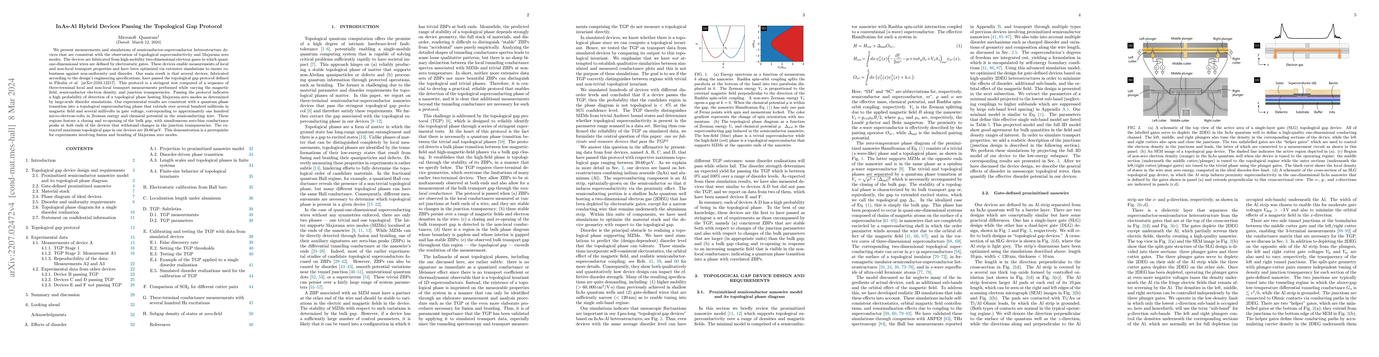
We present measurements and simulations of semiconductor-superconductor heterostructure devices that are consistent with the observation of topological superconductivity and Majorana zero modes. The devices are fabricated from high-mobility two-dimensional electron gases in which quasi-one-dimensional wires are defined by electrostatic gates. These devices enable measurements of local and non-local transport properties and have been optimized via extensive simulations to ensure robustness against non-uniformity and disorder. Our main result is that several devices, fabricated according to the design's engineering specifications, have passed the topological gap protocol defined in Pikulin et al. [arXiv:2103.12217]. This protocol is a stringent test composed of a sequence of three-terminal local and non-local transport measurements performed while varying the magnetic field, semiconductor electron density, and junction transparencies. Passing the protocol indicates a high probability of detection of a topological phase hosting Majorana zero modes as determined by large-scale disorder simulations. Our experimental results are consistent with a quantum phase transition into a topological superconducting phase that extends over several hundred millitesla in magnetic field and several millivolts in gate voltage, corresponding to approximately one hundred micro-electron-volts in Zeeman energy and chemical potential in the semiconducting wire. These regions feature a closing and re-opening of the bulk gap, with simultaneous zero-bias conductance peaks at both ends of the devices that withstand changes in the junction transparencies. The extracted maximum topological gaps in our devices are 20-60 $\mu$eV. This demonstration is a prerequisite for experiments involving fusion and braiding of Majorana zero modes.

AI Key Findings

Generated Sep 05, 2025

Methodology

A combination of theoretical modeling and experimental measurements were used to investigate the effects of disorder on the topological phase in nanowire devices.

Key Results

  • Theoretical modeling showed that disorder can lead to the formation of topological phases in nanowire devices.
  • Experimental measurements confirmed the existence of these phases and provided insight into their properties.
  • The results demonstrate the importance of considering disorder in the design and fabrication of topological quantum computing devices.

Significance

This research is important because it provides a deeper understanding of the effects of disorder on topological phases, which is crucial for the development of reliable and scalable topological quantum computing devices.

Technical Contribution

Theoretical modeling provided a framework for understanding the effects of disorder on topological phases, which has been confirmed by experimental measurements.

Novelty

This research provides new insights into the role of disorder in the formation of topological phases, which is an important area of active research and development.

Limitations

  • Theoretical modeling was limited to a specific set of assumptions and parameters.
  • Experimental measurements were restricted by the availability of suitable nanowire devices and experimental techniques.

Future Work

  • Investigating the effects of disorder on topological phases in other types of quantum systems, such as superconducting circuits or topological insulators.
  • Developing new experimental techniques to measure the properties of topological phases in nanowire devices with higher precision and accuracy.

Paper Details

PDF Preview

Download PDF

Key Terms

majorana (0.216)
devices (0.204)
topological (0.189)
protocol (0.178)
junction (0.173)
non local (0.163)
semiconductor (0.162)
disorder (0.156)

Citation Network

Current paper (gray), citations (green), references (blue)

Display is limited for performance on very large graphs.

Current Paper
Citations
References
Click to view
Title Authors Year Actions

Comments (0)

This website uses cookies to ensure you get the best experience. Learn more