Increasing the Collection Efficiency in Selenium Thin-Film Solar Cells Using a Closed-Space Annealing Strategy
Publication
Metrics
AI Quick Summary
This study introduces a closed-space annealing strategy to optimize the crystallization of selenium thin-film solar cells, enhancing collection efficiency and device performance. The method suppresses selenium sublimation, allowing higher temperature annealing, which reduces charge transfer resistance and improves photovoltaic outcomes.
Paper Preview
Abstract
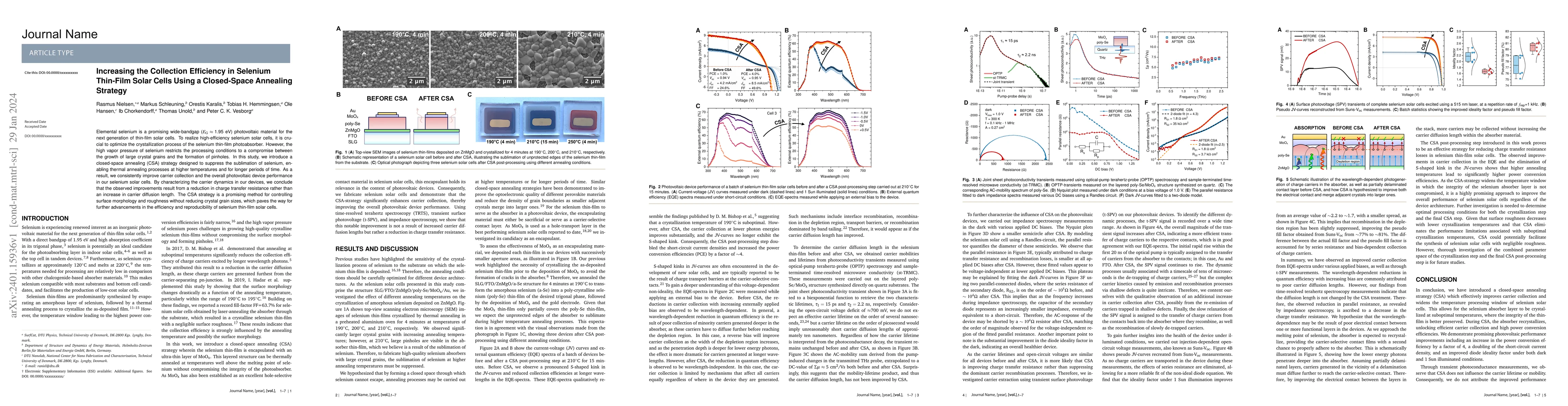
Elemental selenium is a promising wide-bandgap ($E_\mathrm{G}\approx$ 1.95 eV) photovoltaic material for the next generation of thin-film solar cells. To realize high-efficiency selenium solar cells, it is crucial to optimize the crystallization process of the selenium thin-film photoabsorber. However, the high vapor pressure of selenium restricts the processing conditions to a compromise between the growth of large crystal grains and the formation of pinholes. In this study, we introduce a closed-space annealing (CSA) strategy designed to suppress the sublimation of selenium, enabling thermal annealing processes at higher temperatures and for longer periods of time. As a result, we consistently improve carrier collection and the overall photovoltaic device performance in our selenium solar cells. By characterizing the carrier dynamics in our devices, we conclude that the observed improvements result from a reduction in charge transfer resistance rather than an increase in carrier diffusion length. The CSA strategy is a promising method for controlling surface morphology and roughness without reducing crystal grain sizes, which paves the way for further advancements in the efficiency and reproducibility of selenium thin-film solar cells.
AI Key Findings
Get AI-generated insights about this paper's methodology, results, significance, and more — seven facets brought into focus.
Impact
Paper Details
Authors
PDF Preview
Key Terms
Citation Network
Current paper (gray), citations (green), references (blue)
Display is limited for performance on very large graphs.
Discussion 0