Summary
Scalable and cost-effective methods for processing transparent electrodes at the microscale are transversal for advancing in electrochemistry, optoelectronics, microfluidics, and energy harvesting. In these fields, the precise fabrication of micrometric circuits plays a critical role in determining device performance and integration with added-value substrates. In this context, Laser Subtractive Manufacturing stands out among microfabrication techniques for its adaptability to diverse materials and complex configurations, as well as its straightforward scalability and affordability nature. However, a challenge in micromachining metals and metal oxides is the inherent formation of LIPSS, which can significantly impair electrical conductivity, particularly when circuit dimensions fall within the micrometer range. Herein, we investigate the micromachining of TCOs using ultrashort pulse laser systems applied to ITO thin films. We analyze the formation of LIPSS at the edges of the micromachined regions associated with the Gaussian distribution of the energy within the laser spot and their impact on the electrical properties depending on the circuit characteristics. Thus, we evaluate the influence of LIPSS orientation and periodicity by fabricating various circuit patterns using femtosecond lasers at green (515 nm) and ultraviolet (343 nm) wavelengths. A correlation between electrical resistivity measurements and structural analysis reveals distinct effects of nanostructure formation depending on the laser source. For green wavelength, the regions where LIPSS are oriented perpendicular to the ITO track exhibit higher resistance, by a factor just above two, compared to those where LIPSS are parallel. Additionally, UV laser processing results in a pronounced reduction of ITO thickness at the boundary between the LIPSS region and the substrate.
AI Key Findings
Generated Oct 05, 2025
Methodology
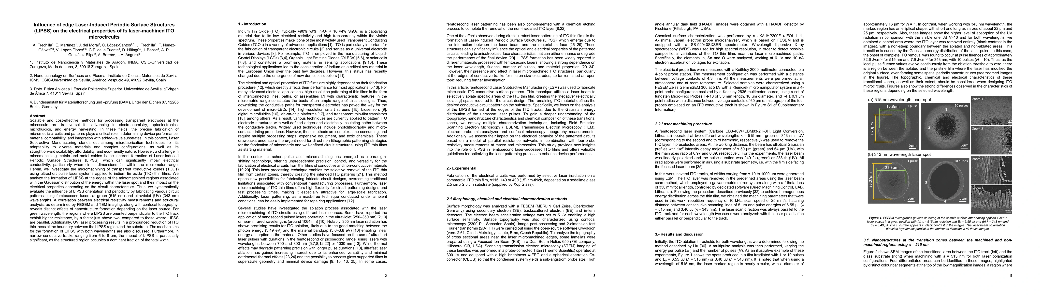
The study employed femtosecond laser machining to create microcircuits on ITO films, combined with high-resolution electrical measurements using a 4-point probe system to analyze the impact of laser-induced periodic surface structures (LIPSS) on electrical properties.
Key Results
- LIPSS orientation significantly affects the anisotropic resistivity of ITO films, with parallel structures causing higher resistance compared to perpendicular ones.
- UV laser processing (343 nm) produced more regular and uniform nanostructures than green laser (515 nm) processing, leading to better electrical performance.
- The spatial periodicity of LIPSS was quantified using 2D-FFT analysis, revealing a direct correlation between structure periodicity and electrical conductivity.
Significance
This research provides critical insights into how nanoscale surface modifications via laser processing can control electrical properties of transparent conductive materials, with implications for advanced optoelectronic devices and flexible electronics.
Technical Contribution
The work introduces a systematic approach to correlate laser-induced nanostructuring with electrical behavior, utilizing advanced 2D-FFT analysis and high-resolution microprobe measurements.
Novelty
This study uniquely combines femtosecond laser processing with detailed electrical characterization to demonstrate how controlled nanoscale surface patterns can be used to engineer anisotropic resistivity in transparent conductive films.
Limitations
- The study focused on specific laser parameters and ITO thicknesses, limiting generalizability to other materials or conditions.
- Electrical measurements were conducted on flat surfaces, excluding potential effects of curved or 3D geometries.
Future Work
- Investigate the effect of varying laser wavelengths and pulse durations on LIPSS formation and electrical properties.
- Explore the integration of LIPSS-based resistivity control in flexible and wearable electronics applications.
- Develop predictive models linking LIPSS periodicity to electrical conductivity for design optimization.
Comments (0)