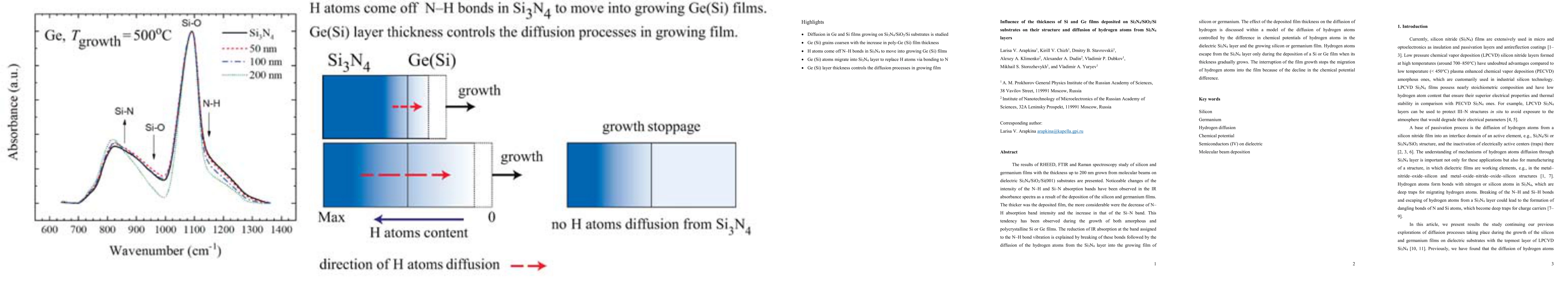
Diffusion processes in germanium and silicon films grown on Si3N4 substrates
|
L. V. Arapkina, K. Chizh, D. Stavrovskii, V. Dubkov, E. P. Lazareva, V. Yuryev
|
2020
|
View Paper
|
Charge transport mechanism and amphoteric nature of traps in amorphous silicon nitride
|
Y. Novikov, V. Gritsenko
|
2020
|
View Paper
|
Development of advanced hydrogenation processes for silicon solar cells via an improved understanding of the behaviour of hydrogen in silicon
|
B. Hallam, P. Hamer, Alison M. Ciesla née Wenham, Catherine E. Chan, Bruno Vicari Stefani, S. Wenham
|
2020
|
View Paper
|
Growth and Characterization of Undoped Polysilicon Thick Layers: Revisiting an Old System
|
Taguhi Yeghoyan, Kassem Alassaad, V. Souliere, T. Douillard, D. Carole, G. Ferro
|
2019
|
View Paper
|
Diffusion of hydrogen atoms in silicon layers deposited from molecular beams on dielectric substrates
|
K. Chizh, L. V. Arapkina, D. B. Stavrovsky, P. Gaiduk, V. Yuryev
|
2019
|
View Paper
|
Dielectric surface passivation for silicon solar cells: A review
|
R. S. Bonilla, B. Hoex, P. Hamer, P. Wilshaw
|
2017
|
View Paper
|
Silicon-germanium and platinum silicide nanostructures for silicon based photonics
|
M. S. Storozhevykh, V. Dubkov, L. V. Arapkina, K. Chizh, S. Mironov, V. A. Chapnin, V. Yuryev
|
2017
|
View Paper
|
Hydrogen incorporation, stability, and release effects in thin film silicon
|
W. Beyer
|
2016
|
View Paper
|
Si3N4 layers for the in-situ passivation of GaN-based HEMT structures
|
P. Yunin, Y. Drozdov, M. Drozdov, S. A. Korolev, A. Okhapkin, O. Khrykin, V. Shashkin
|
2015
|
View Paper
|
Raman Characterization of Poly-Si Channel Materials for 3D Flash Memory Device Applications
|
W. Yoo, T. Ishigaki, T. Ueda, K. Kang, D. Sheen, Sung Soon Kim, M. Ko, W. S. Shin, N. Kwak, Byung-Seok Lee
|
2014
|
View Paper
|
Advances in surface passivation and emitter optimization techniques of c-Si solar cells
|
M. Rahman
|
2014
|
View Paper
|
Detailed Micro Raman Spectroscopy Analysis of Doped Silicon Thin Film Layers and Its Feasibility for Heterojunction Silicon Wafer Solar Cells
|
Z. Ling, J. Ge, R. Stangl, A. Aberle, T. Mueller
|
2013
|
View Paper
|
Micro-Raman characterization of Germanium thin films evaporated on various substrates
|
V. Sorianello, L. Colace, G. Assanto, M. Nardone
|
2011
|
View Paper
|
Raman characterization of the structural evolution in amorphous and partially nanocrystalline hydrogenated silicon thin films prepared by PECVD
|
Zhi Li, Wei Li, Yadong Jiang, Haihong Cai, Yuguang Gong, Jian He
|
2011
|
View Paper
|
Microstructure and photovoltaic performance of polycrystalline silicon thin films on temperature-stable ZnO:Al layers
|
C. Becker, F. Ruske, T. Sontheimer, B. Gorka, U. Bloeck, S. Gall, B. Rech
|
2009
|
View Paper
|
Analysis of Carrier Traps in Silicon Nitride Film with Discharge Current Transient Spectroscopy, Photoluminescence, and Electron Spin Resonance
|
H. Aozasa, I. Fujiwara, Y. Kamigaki
|
2007
|
View Paper
|
Bulk and surface passivation of silicon solar cells accomplished by silicon nitride deposited on industrial scale by microwave PECVD
|
W. Soppe, H. Rieffe, A. Weeber
|
2005
|
View Paper
|
Improvement of AlGaN∕GaN high electron mobility transistor structures by in situ deposition of a Si3N4 surface layer
|
J. Derluyn, S. Boeykens, K. Cheng, R. Vandersmissen, J. Das, W. Ruythooren, S. Degroote, M. Leys, M. Germain, G. Borghs
|
2005
|
View Paper
|
Low-temperature Si growth on Si (001): Impurity incorporation and limiting thickness for epitaxy
|
J. Baribeau, X. Wu, D. J. Lockwood, L. Tay, G. Sproule
|
2004
|
View Paper
|
Raman and transmission electron microscopy study of disordered silicon grown by molecular beam epitaxy
|
L. Tay, D. J. Lockwood, J. Baribeau, X. Wu, G. Sproule
|
2004
|
View Paper
|
Relationship between Raman crystallinity and open-circuit voltage in microcrystalline silicon solar cells
|
C. Droz, E. Vallat-Sauvain, J. Bailat, L. Feitknecht, J. Meier, Arvind Shah
|
2004
|
View Paper
|
Diffusion and evolution of hydrogen in hydrogenated amorphous and microcrystalline silicon
|
W. Beyer
|
2003
|
View Paper
|
Arrangement of Si and O Atoms in Thermally Grown SiO2 Films
|
D. Davazoglou, V. Vamvakas
|
2003
|
View Paper
|
Study of structure and quality of different silicon oxides using FTIR and Raman microscopy
|
C. Moore, T. Perova, B. J. Kennedy, K. Berwick, I. Shaganov, R. Moore
|
2003
|
View Paper
|
Grain Growth in Polycrystalline Thin Films of Semiconductors
|
C. Thompson
|
1998
|
View Paper
|
Incorporation and thermal stability of hydrogen in amorphous silicon and germanium
|
W. Beyer
|
1996
|
View Paper
|
The relationship between hydrogen and electronic defects in amorphous silicon
|
S. Deane, M. J. Powell
|
1996
|
View Paper
|
Nature of the Si and N dangling bonds in silicon nitride
|
J. Robertson, W. L. Warren, J. Kanicki
|
1995
|
View Paper
|
Silicon-hydrogen bonding and hydrogen diffusion in amorphous silicon.
|
Van de Walle Cg, R. Street
|
1995
|
View Paper
|
Defects and hydrogen in amorphous silicon nitride
|
J. Robertson
|
1994
|
View Paper
|
Hydrogen migration and electronic carriers in a-Si:H.
|
Santos, Johnson, Street, Hack, Thompson, Tsai
|
1993
|
View Paper
|
Hydrogen diffusion in polycrystalline silicon thin films
|
W. Jackson, N. Johnson, C. Tsai, I. Wu, A. Chiang, D. L. Smith
|
1992
|
View Paper
|
Hydrogen transport in amorphous silicon.
|
Jackson, Tsai
|
1992
|
View Paper
|
Hydrogen chemical potential and structure of a-Si:H.
|
Street
|
1991
|
View Paper
|
Raman scattering and short range order in amorphous germanium
|
J. Lannin, N. Maley, S. Kshirsagar
|
1985
|
View Paper
|
Nitrogen-bonding environments in glow-discharge—deposited a − Si : H films
|
G. Lucovsky, Jeffrey Yang, S. Chao, J. Tyler, W. Czubatyj
|
1983
|
View Paper
|
The one phonon Raman spectrum in microcrystalline silicon
|
H. Richter, Z. P. Wang, L. Ley
|
1981
|
View Paper
|
Raman scattering from small particle size polycrystalline silicon
|
Z. Iqbal, S. Vepřek, A. Webb, P. Capezzuto
|
1981
|
View Paper
|
The hydrogen content of plasma‐deposited silicon nitride
|
W. Lanford, M. Rand
|
1978
|
View Paper
|
Infrared and Raman spectra of the silicon-hydrogen bonds in amorphous silicon prepared by glow discharge and sputtering
|
M. Brodsky, M. Cardona, J. Cuomo
|
1977
|
View Paper
|
Adiabatic bond charge model for the phonons in diamond, Si, Ge, and α-Sn
|
W. Weber
|
1977
|
View Paper
|
Hydrogen content and annealing of memory quality silicon-oxynitride films
|
H. Stein
|
1976
|
View Paper
|
Multiphonon Raman Spectrum of Silicon
|
P. Temple, C. E. Hathaway
|
1973
|
View Paper
|
Characterization of Silicon Nitride Films
|
E. Taft
|
1971
|
View Paper
|
Raman Scattering by Silicon and Germanium
|
J. Parker, D. Feldman, M. Ashkin
|
1967
|
View Paper
|
Infrared studies on polymorphs of silicon dioxide and germanium dioxide
|
Ellis, Lippincott, A. V. Valkenburg, Charles E. Weir, Elmer N. Bunting
|
1958
|
View Paper
|
Intrinsic Optical Absorption in Single-Crystal Germanium and Silicon at 77°K and 300°K
|
W. C. Dash, R. Newman
|
1955
|
View Paper
|
Disorder and defect formation mechanisms in molecular-beam-epitaxy grown silicon epilayers
|
A. Akbari-Sharbaf, J. Baribeau, Xiaohua Wu, D. J. Lockwood, G. Fanchini
|
2013
|
View Paper
|
Hydrogen stability in amorphous germanium films
|
W. Beyer, J. Herion, H. Wagner, U. Zastrow
|
1991
|
View Paper
|
Yuryev, Diffusion processes in germanium and silicon films grown on Si3N4 substrates, Sol
|
|
2021
|
|
Czubatyj, Nitrogen-bonding environments in glow-discharge –deposited a-Si:H films
|
|
1983
|
|
Real-time observation of initial stages of copper film growth on siliconoxide using reflection high-energy electron diffraction
|
|
2004
|
|
Arapkina: Investigation, Data Curation, Writing -Original Draft
|
|
|
|
Si 3 N 4 layers for the in - situ passivation of GaN - based HEMT structures Advances in surface passivation and emitter optimization techniques of cSi solar cells
|
|
2014
|
|
a review, Phys
|
|
2017
|
|
Impurity incorporation and limiting thickness for epitaxy, J
|
|
2004
|
|
Effect of oxygen pressure on the texture of a magnetite film grown by reactive deposition on a SiO 2 /Si(001) surface
|
|
2015
|
|
Yuryev, Silicon-germanium and platinum silicides nanostructures for silicon based photonics
|
|
2017
|
|
Quantitative determination of hydrogen in siliconnitride films using proton scattering
|
|
1980
|
|
Sproule, Raman and transmission electron microscopy study of disordered silicon grown by molecular beam epitaxy
|
|
2004
|
|
Chizh: Investigation, Data Curation, Writing -Original Draft
|
|
|
|
Storozhevykh: Investigation, Data Curation, Writing -Original Draft
|
|
|
|
Growth and characterization of undoped polysilicon thick layers: revisiting an old system, Silicon
|
|
1900
|
|
Korobtsova, Effect of oxygen pressure on the texture of a magnetite film grown by reactive deposition on a SiO2/Si(001) surface
|
|
2015
|
|
Shashkin, Si3N4 layers for the in-situ passivation of GaN-based HEMT structures, Semiconductors
|
|
2015
|
|
Comments (0)