ArxivLens
ArXiv physics.app-ph cond-mat.mtrl-sci physics.optics

InGaN Nanopixel Arrays on Single Crystal GaN Substrate

Christy Giji Jenson, Dipon Kumar Ghosh, Grzegorz Muziol, Md Zunaid Baten, Nirmal Anand, Pei-Cheng Ku, Sadat Tahmeed Azad, Sharif Sadaf

2506.11408 Published Jun 13, 2025
View PDF

Publication

Published: Jun 13, 2025
Updated: Aug 04, 2025
Categories: physics.app-ph, cond-mat.mtrl-sci, physics.optics

Metrics

Source: ArXiv

Quick Answers

What methodology did the authors use?

This research employed a combination of experimental and theoretical techniques to investigate the properties of InGaN nanopixel arrays. More in Methodology →

What are the key results?

The nanopixels exhibited a high external quantum efficiency (EQE) of up to 42% at low injection currents. — A blueshift of approximately 14 nm was observed as the injection current density increased. More in Key Results →

Why is this work significant?

This research contributes to our understanding of the properties and potential applications of InGaN nanopixel arrays, which may enable more efficient and compact display devices. More in Significance →

What are the main limitations?

The study was limited by the small sample size and the need for further optimization of the fabrication process. — The experimental setup did not allow for precise control over the injection current density. More in Limitations →

Paper Preview

Abstract

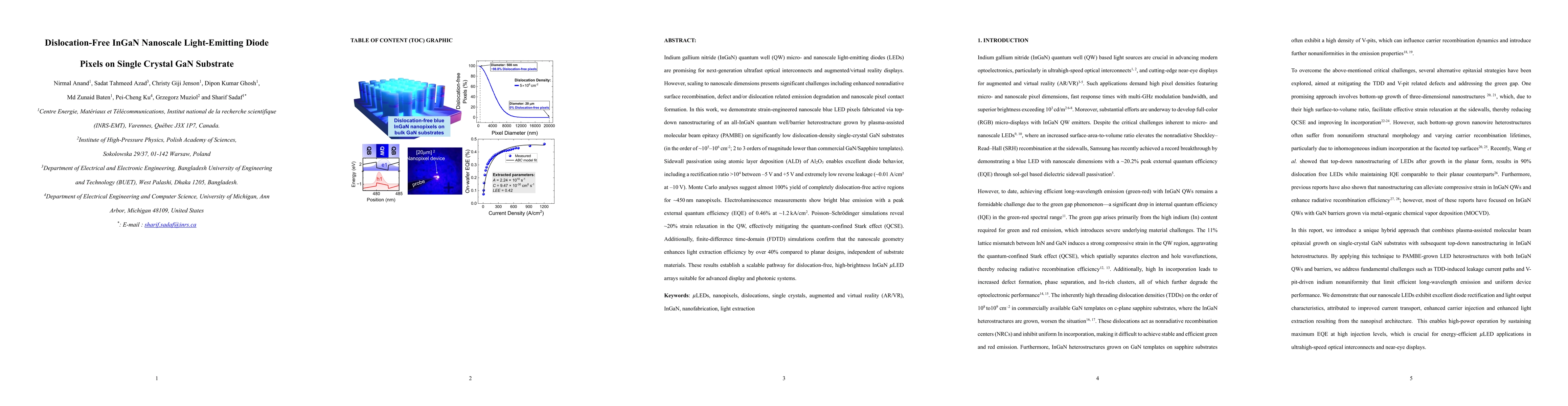
Indium gallium nitride (InGaN) quantum well (QW) micro- and nano-scale light-emitting diodes (LEDs) are vital to the next-generation optoelectronic applications such as ultrahigh-speed optical interconnects and near-eye augmented/virtual reality displays. However, scaling to nanoscale dimensions introduces several challenges, including an increased nonradiative recombination from surface states and defect-related emission degradation. In this work, we present a high-performance, strain-relaxed nanoscale LED array, fabricated using a top-down nanostructuring approach applied to a high-quality, all-InGaN (quantum well/barrier) LED structure grown by plasma-assisted molecular beam epitaxy (PAMBE) on bulk GaN substrates. Combining an ultra-low threading dislocation density bulk GaN substrate and effective sidewall passivation with atomic layer deposition (ALD) results in excellent diode rectification characteristics and extremely low leakage currents. Electroluminescence measurements reveal bright blue emission with a peak external quantum efficiency (EQE) of 0.46% at an elevated injection current density of ~1.2 kA/cm2.

Key Findings, in focus

Seven facets of this paper, analysed and brought into focus by AI.

AI-generated · verify against source Generated Sep 06, 2025
In focus · one-line synthesis

This research contributes to our understanding of the properties and potential applications of InGaN nanopixel arrays, which may enable more efficient and compact display devices.

01
MethodologyHow they did it

This research employed a combination of experimental and theoretical techniques to investigate the properties of InGaN nanopixel arrays.

02
ResultsWhat they found
  • The nanopixels exhibited a high external quantum efficiency (EQE) of up to 42% at low injection currents.
  • A blueshift of approximately 14 nm was observed as the injection current density increased.
  • The light extraction efficiency (LEE) of the nanopixel arrays was found to be significantly higher than that of planar structures.
03
SignificanceWhy it matters

This research contributes to our understanding of the properties and potential applications of InGaN nanopixel arrays, which may enable more efficient and compact display devices.

04
Technical ContributionsWhat's new technically

The development of a novel fabrication process for InGaN nanopixel arrays, which enabled the creation of high-quality devices with improved performance characteristics.

05
NoveltyWhat sets it apart

This research presents a new approach to the design and fabrication of InGaN nanopixel arrays, which may enable more efficient and compact display devices.

06
LimitationsWhat to be cautious about
  • The study was limited by the small sample size and the need for further optimization of the fabrication process.
  • The experimental setup did not allow for precise control over the injection current density.
07
Future WorkWhere it goes next
  • Investigating the effects of different substrate materials on the performance of InGaN nanopixel arrays.
  • Developing more efficient fabrication methods to improve the yield and uniformity of the nanopixels.

Impact

6
References

Paper Details

Paper ID: 2506.11408
Categories:
physics.app-ph cond-mat.mtrl-sci physics.optics

How to Cite This Paper

Reference manager: RIS EndNote


Discussion 0

This website uses cookies to ensure you get the best experience. Learn more