Publication
Metrics
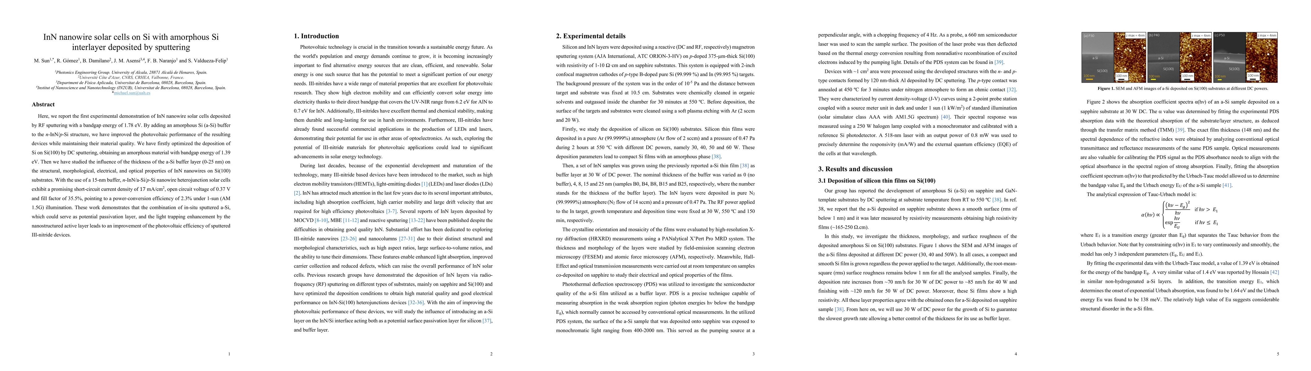
Paper Preview
Abstract
Here, we report the first experimental demonstration of InN nanowire solar cells deposited by RF sputtering with a bandgap energy of 1.78 eV. By adding an amorphous Si (a-Si) buffer to the n-InN/p-Si structure, we have improved the photovoltaic performance of the resulting devices while maintaining their material quality. We have firstly optimized the deposition of Si on Si(100) by DC sputtering, obtaining an amorphous material with bandgap energy of 1.39 eV. Then we have studied the influence of the thickness of the a-Si buffer layer (0-25 nm) on the structural, morphological, electrical, and optical properties of InN nanowires on Si (100) substrates. With the use of a 15-nm buffer, n-InN/a-Si/p-Si nanowire heterojunction solar cells exhibit a promising short-circuit current density of 17 mA/cm2, open circuit voltage of 0.37 V and fill factor of 35.5%, pointing to a power-conversion efficiency of 2.3% under 1-sun (AM 1.5G) illumination. These work demonstrated that the combination of in-situ sputtered a-Si, which could serve as potential passivation layer, and the light trapping enhancement by the nanostructured active layer leads to an improvement of the photovoltaic efficiency of sputtered III-nitride devices.
AI Key Findings
Get AI-generated insights about this paper's methodology, results, significance, and more — seven facets brought into focus.
Discussion 0