01
MethodologyHow they did it
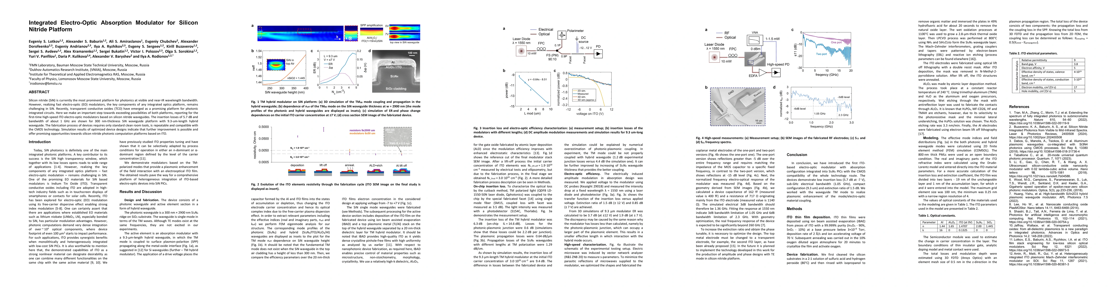
The study fabricated a hybrid silicon‑nitride/ITO waveguide using standard CMOS‑compatible processes (IBAD for ITO, ALD for Al2O3, e‑beam lithography for patterning). 3D FEM and FDTD simulations were performed to design the device and predict optical/electrical performance, followed by experimental characterization of insertion loss, extinction ratio, and high‑speed response using a laser diode, photodetector, and vector network analyzer.
Discussion 0