Integrated on chip platform with quantum emitters in layered materials
Publication
Metrics
AI Quick Summary
This study demonstrates efficient room temperature coupling of quantum emitters embedded in hexagonal boron nitride to an on-chip aluminium nitride waveguide, achieving 1.2% light coupling efficiency and single photon transmission, paving the way for integrated quantum photonic circuitry.
Paper Preview
Abstract
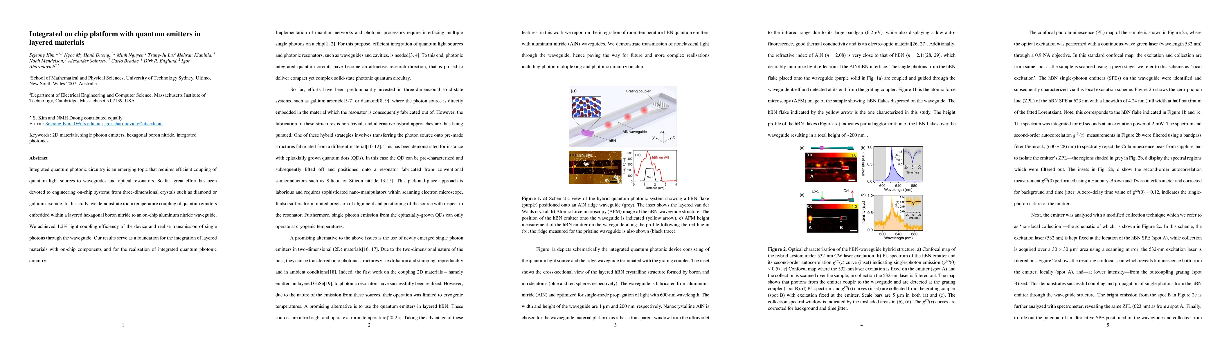
Integrated quantum photonic circuitry is an emerging topic that requires efficient coupling of quantum light sources to waveguides and optical resonators. So far, great effort has been devoted to engineering on-chip systems from three-dimensional crystals such as diamond or gallium arsenide. In this study, we demonstrate room temperature coupling of quantum emitters embedded within a layered hexagonal boron nitride to an on-chip aluminium nitride waveguide. We achieved 1.2% light coupling efficiency of the device and realise transmission of single photons through the waveguide. Our results serve as a foundation for the integration of layered materials with on-chip components and for the realisation of integrated quantum photonic circuitry.
AI Key Findings
Get AI-generated insights about this paper's methodology, results, significance, and more — seven facets brought into focus.
Impact
Paper Details
PDF Preview
Key Terms
Citation Network
Current paper (gray), citations (green), references (blue)
Display is limited for performance on very large graphs.
Discussion 0