The research proposes leveraging anisotropy in 2D materials to tailor modal fields supported by 2D material waveguides, enabling improved efficiencies for coupling-based photonic functions.
Integrated Photonic Functions Using Anisotropic 2D Material Structures
Publication
Metrics
AI Quick Summary
This paper proposes leveraging the anisotropy of 2D materials to tailor modal fields in 2D plasmonic waveguides, enabling them to mimic the functionality of 3D dielectric waveguides and enhancing photonic device capabilities. The use of materials like black phosphorus allows for improved coupling-based functions and the potential for 2D plasmonic circuits.
Quick Answers
What methodology did the authors use?
The research proposes leveraging anisotropy in 2D materials to tailor modal fields supported by 2D material waveguides, enabling improved efficiencies for coupling-based photonic functions. More in Methodology →
What are the key results?
Anisotropic 2D materials can localize modal fields around waveguide centers, mimicking the oscillatory nature of 3D dielectric waveguides. — This approach enhances the efficiencies of in-plane multimode-interference couplers and out-of-plane optical radiation. More in Key Results →
Why is this work significant?
This research is significant as it introduces a novel approach to tailor modal fields in 2D material waveguides, unlocking beneficial design advantages in 2D plasmonics not achievable in isotropic counterparts. More in Significance →
What are the main limitations?
The study is limited to theoretical analysis and simulations, with practical experimental validation required for real-world applications. — Material properties and performance may vary based on fabrication techniques and material quality. More in Limitations →
Abstract
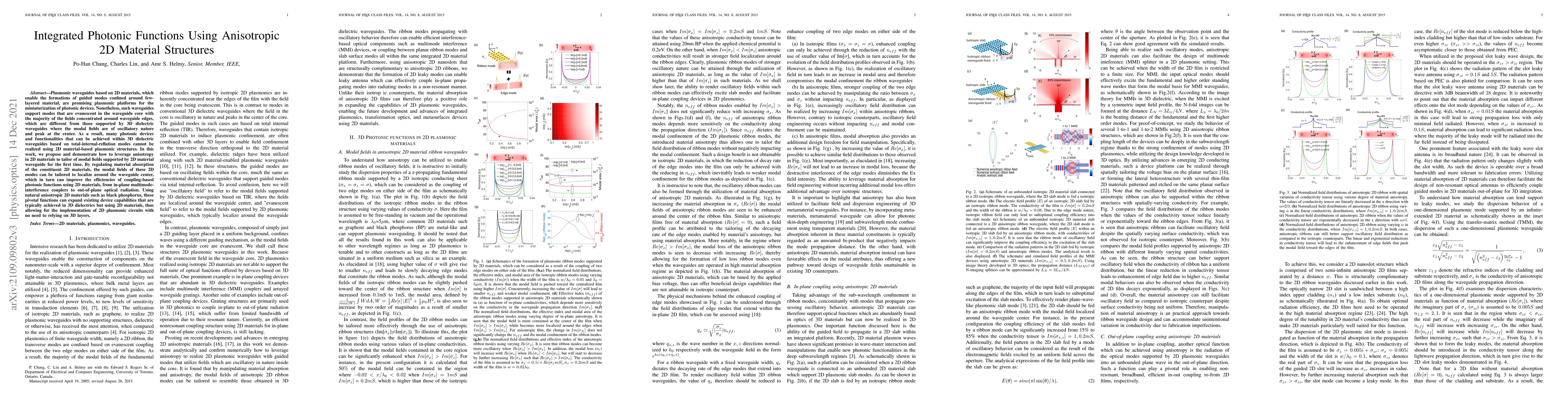
Plasmonic waveguides based on 2D materials, which enable the formations of guided modes confined around few-layered material, are promising plasmonic platforms for the miniaturization of photonic devices. Nonetheless, such waveguides support modes that are evanescent in the waveguide core with the majority of the fields concentrated around waveguide edges, which are different from those supported by 3D dielectric waveguides where the modal fields are of oscillatory nature and peak at the center. As a result, many photonic devices and functionalities that can be achieved within 3D dielectric waveguides based on total-internal-reflation modes cannot be realized using 2D material-based plasmonic structures. In this work, we propose and demonstrate how to leverage anisotropy in 2D materials to tailor of modal fields supported by 2D material waveguide for the first time. By regulating material absorption of the constituent 2D materials, the modal fields of these 2D modes can be tailored to localize around the waveguide center, which in turn can improve the efficiencies of coupling-based photonic functions using 2D materials, from in-plane multimode-interference couplers to out-of-plane optical radiation. Using natural anisotropic 2D materials such as black phosphorus, these pivotal functions can expand existing device capabilities that are typically achieved in 3D dielectrics but using 2D materials, thus allowing for the implementation of 2D plasmonic circuits with no need to relying on 3D layers.
Key Findings, in focus
Seven facets of this paper, analysed and brought into focus by AI.
This research is significant as it introduces a novel approach to tailor modal fields in 2D material waveguides, unlocking beneficial design advantages in 2D plasmonics not achievable in isotropic counterparts.
- Anisotropic 2D materials can localize modal fields around waveguide centers, mimicking the oscillatory nature of 3D dielectric waveguides.
- This approach enhances the efficiencies of in-plane multimode-interference couplers and out-of-plane optical radiation.
- Natural anisotropic 2D materials, such as black phosphorus, can expand device capabilities typically achieved in 3D dielectrics without relying on 3D layers.
- Anisotropic 2D materials offer design capabilities not attainable in isotropic counterparts, allowing for the implementation of 2D plasmonic circuits.
- The study demonstrates that anisotropy can facilitate field and dispersion engineering of 3D metamaterial waveguides, enabling photonics skin-depth engineering and subwavelength mode confinement using transparent materials.
This research is significant as it introduces a novel approach to tailor modal fields in 2D material waveguides, unlocking beneficial design advantages in 2D plasmonics not achievable in isotropic counterparts.
The paper presents a method to leverage anisotropy in 2D materials for tailoring modal fields in waveguides, improving coupling efficiencies for photonic functions.
The novelty of this work lies in its approach to utilizing the inherent anisotropy of 2D materials to achieve modal field localization and oscillatory behavior, similar to 3D dielectric waveguides, thereby expanding the capabilities of 2D plasmonic devices.
- The study is limited to theoretical analysis and simulations, with practical experimental validation required for real-world applications.
- Material properties and performance may vary based on fabrication techniques and material quality.
- Further experimental validation and optimization of anisotropic 2D material-based photonic devices.
- Exploration of additional anisotropic 2D materials for enhanced performance and broader applicability.
Impact
Paper Details
Authors
PDF Preview
Key Terms
Citation Network
Current paper (gray), citations (green), references (blue)
Display is limited for performance on very large graphs.
Discussion 0