Integrating high-quality dielectrics with one-nanometer equivalent oxide thickness on two-dimensional electronic devices
Publication
Metrics
AI Quick Summary
This paper reports the successful integration of high-quality, ultrathin dielectrics on two-dimensional semiconductors using atomic layer deposition with a 0.3 nm-thick monolayer molecular crystal seeding layer, achieving a 1 nm equivalent oxide thickness with reduced leakage and improved transistor performance. The method is shown to be effective across various 2D materials, enabling high-frequency graphene RF transistors and low-voltage CMOS transistors.
Paper Preview
Abstract
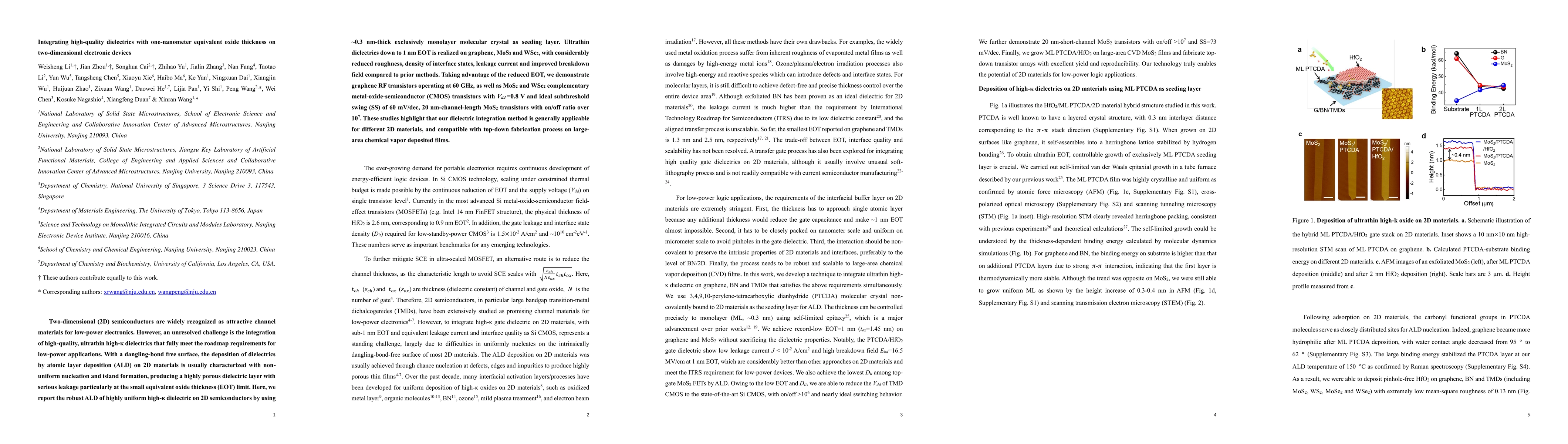
Two-dimensional (2D) semiconductors are widely recognized as attractive channel materials for low-power electronics. However, an unresolved challenge is the integration of high-quality, ultrathin high-\k{appa} dielectrics that fully meet the roadmap requirements for low-power applications. With a dangling-bond free surface, the deposition of dielectrics by atomic layer deposition (ALD) on 2D materials is usually characterized with non-uniform nucleation and island formation, producing a highly porous dielectric layer with serious leakage particularly at the small equivalent oxide thickness (EOT) limit. Here, we report the robust ALD of highly uniform high-\k{appa} dielectric on 2D semiconductors by using ~0.3 nm-thick exclusively monolayer molecular crystal as seeding layer. Ultrathin dielectrics down to 1 nm EOT is realized on graphene, MoS2 and WSe2, with considerably reduced roughness, density of interface states, leakage current and improved breakdown field compared to prior methods. Taking advantage of the reduced EOT, we demonstrate graphene RF transistors operating at 60 GHz, as well as MoS2 and WSe2 complementary metal-oxide-semiconductor (CMOS) transistors with Vdd =0.8 V and ideal subthreshold swing (SS) of 60 mV/dec, 20 nm-channel-length MoS2 transistors with on/off ratio over 10^7. These studies highlight that our dielectric integration method is generally applicable for different 2D materials, and compatible with top-down fabrication process on large-area chemical vapor deposited films.
AI Key Findings
Get AI-generated insights about this paper's methodology, results, significance, and more — seven facets brought into focus.
Impact
Paper Details
Authors
PDF Preview
Key Terms
Citation Network
Current paper (gray), citations (green), references (blue)
Display is limited for performance on very large graphs.
Discussion 0