Quick Summary:

This paper presents a novel method for depositing films of various van der Waals materials on paper substrates by rubbing vdW crystals against the paper, exploiting weak interlayer interactions. The study demonstrates the high optical quality and exceptionally low electrical resistivity of these films, showcasing their potential for low-cost, environmentally friendly electronic and optical applications.

Summary

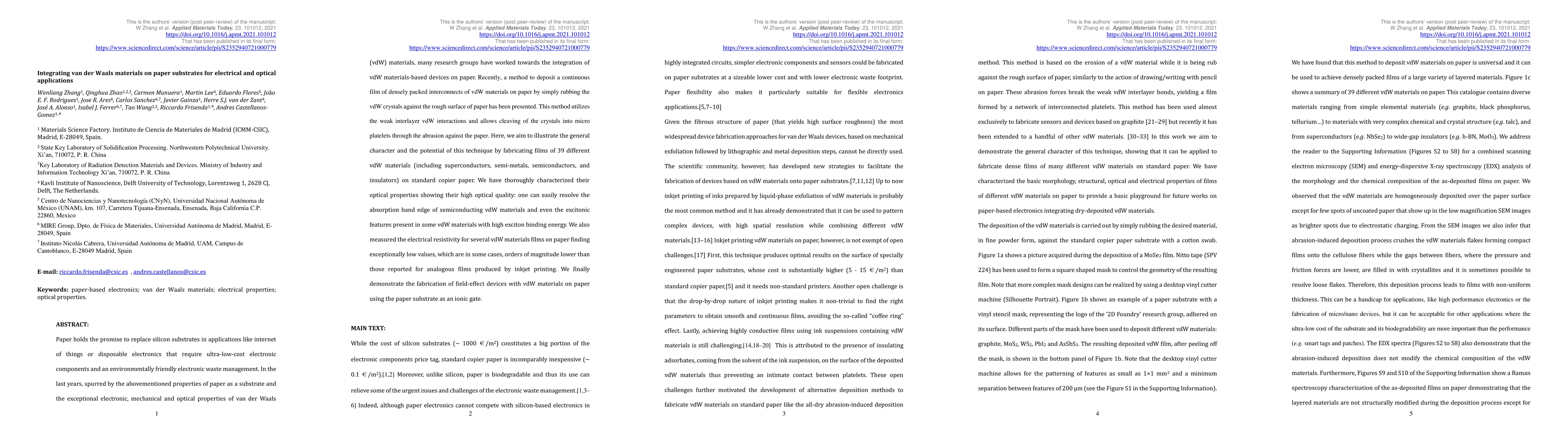
Paper holds the promise to replace silicon substrates in applications like internet of things or disposable electronics that require ultra-low-cost electronic components and an environmentally friendly electronic waste management. In the last years, spurred by the abovementioned properties of paper as a substrate and the exceptional electronic, mechanical and optical properties of van der Waals (vdW) materials, many research groups have worked towards the integration of vdW materials-based devices on paper. Recently, a method to deposit a continuous film of densely packed interconnects of vdW materials on paper by simply rubbing the vdW crystals against the rough surface of paper has been presented. This method utilizes the weak interlayer vdW interactions and allows cleaving of the crystals into micro platelets through the abrasion against the paper. Here, we aim to illustrate the general character and the potential of this technique by fabricating films of 39 different vdW materials (including superconductors, semi-metals, semiconductors, and insulators) on standard copier paper. We have thoroughly characterized their optical properties showing their high optical quality: one can easily resolve the absorption band edge of semiconducting vdW materials and even the excitonic features present in some vdW materials with high exciton binding energy. We also measured the electrical resistivity for several vdW materials films on paper finding exceptionally low values, which are in some cases, orders of magnitude lower than those reported for analogous films produced by inkjet printing. We finally demonstrate the fabrication of field-effect devices with vdW materials on paper using the paper substrate as an ionic gate.

AI Key Findings

Get AI-generated insights about this paper's methodology, results, and significance.

Paper Details

PDF Preview

Download PDF

Key Terms

materials (0.263)
materials (0.246)
films (0.220)
films (0.214)
substrate (0.192)
electronic (0.190)
optical properties (0.189)
substrate (0.188)
crystals (0.186)
electronic (0.172)
crystals (0.164)
optical (0.155)
paper (0.146)
devices (0.145)
optical (0.143)
devices (0.143)
paper (0.136)
exciton (0.128)
der (0.123)
excitonic (0.123)

Citation Network

Current paper (gray), citations (green), references (blue)

Current Paper
Citations
References
Click to view
Title Authors Year Actions
Quantitative analysis of printed nanostructured networks using high-resolution 3D FIB-SEM nanotomography
Cian Gabbett, Luke Doolan, Kevin Synnatschke, Laura Gambini, Emmet Coleman, Adam G. Kelly, Shixin Liu, Eoin Caffrey, Jose M Munuera, Catriona Murphy, S. Sanvito, Lewys Jones, Jonathan N. Coleman
2024
View Paper
Van der Waals materials for paper electronics
Wenliang Zhang, Kexin He, Andres Castellanos-Gomez, Yong Xie
2023
View Paper
3D-imaging of Printed Nanostructured Networks using High-resolution FIB-SEM Nanotomography
Cian Gabbett, Luke Doolan, Kevin Synnatschke, Laura Gambini, Emmet Coleman, Adam G. Kelly, Shixin Liu, Eoin Caffrey, J. Munuera, Catriona Murphy, S. Sanvito, L. Jones, J. Coleman
2023
View Paper
Paper-based Flexible Supercapacitors with drawn van der Waals materials
Bahareh Nouri, A. Castellanos-Gomez, Foad Ghasemi
2023
View Paper
Morphology and Luminescence Properties of Cellulose+KBi0.99Pr0.01 (MoO4)2 Composites
V. Chornii, V. Boyko, S. Nedilko, V. Scherbatskyi, Kateryna Terebilenko, P. Teselko, O. Gomenyuk, Vadym Sheludko
2022
View Paper
2D Materials towards sensing technology: From fundamentals to applications
M. V. Sulleiro, Antonio Dominguez-Alfaro, N. Alegret, A. Silvestri, I. J. Gómez
2022
View Paper
Eco-Friendly Disposable WS2 Paper Sensor for Sub-ppm NO2 Detection at Room Temperature
D. Matatagui, C. Cruz, F. Carrascoso, A. Al-Enizi, A. Nafady, A. Castellanos-Gomez, M. C. Horrillo
2022
View Paper
Paper-based printed CPW-fed antenna for Wi-Fi applications
Nitheesh M. Nair, D. Ray, P. Swaminathan
2022
View Paper
Paper-supported WS2 Strain Gauges
Wenliang Zhang, R. Frisenda, Qinghua Zhao, F. Carrascoso, A. Al-Enizi, A. Nafady, A. Castellanos-Gomez
2021
View Paper
Integrating superconducting van der Waals materials on paper substrates†
J. Azpeitia, R. Frisenda, Martin Lee, D. Bouwmeester, Wenliang Zhang, F. Mompeán, H. S. van der Zant, M. Garc'ia-Hern'andez, A. Castellanos-Gomez
2021
View Paper
Solvent-free fabrication of broadband WS2 photodetectors on paper
Wenliang Zhang, O. Çakıroğlu, A. Al-Enizi, A. Nafady, Xuetao Gan, Xiaohua Ma, Sruthi Kuriakose, Yong Xie, A. Castellanos-Gomez
2023
View Paper
Morphological Characterisation of Printed Nanostructured Networks using High-resolution 3D FIB-SEM Nanotomography
View Paper

Comments (0)

This website uses cookies to ensure you get the best experience. Learn more