Publication
Metrics
AI Quick Summary
Researchers used TEM to study atomic number contrast in thick samples, finding that electrons from a high-density material increase signal near interfaces with lower-density materials.
Paper Preview
Abstract
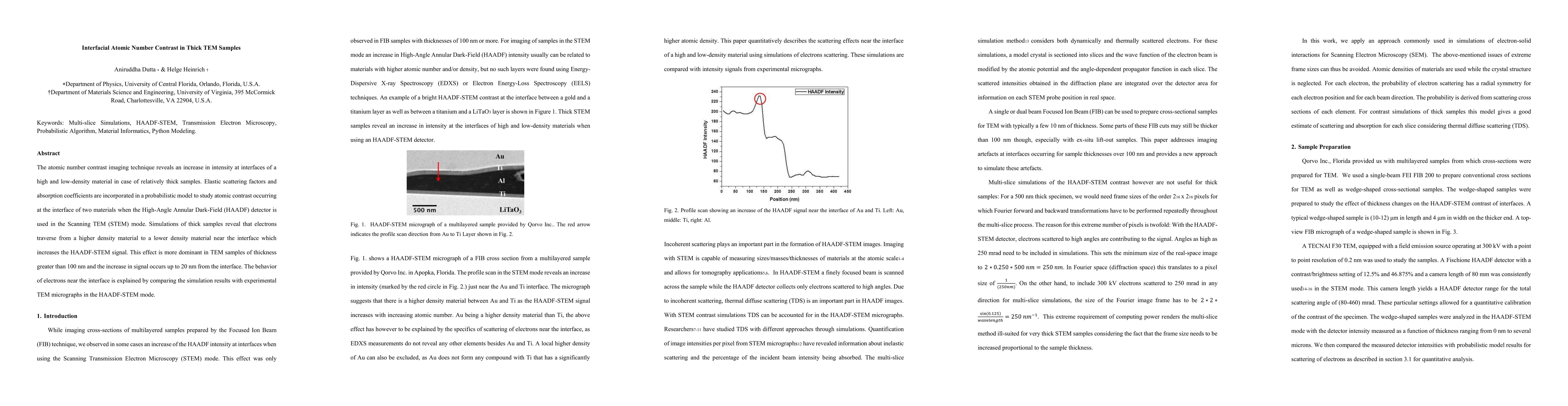
The atomic number contrast imaging technique reveals an increase in intensity at interfaces of a high and low-density material in case of relatively thick samples. Elastic scattering factors and absorption coefficients are incorporated in a probabilistic model to study atomic contrast occurring at the interface of two materials when the High-Angle Annular Dark-Field (HAADF) detector is used in the Scanning TEM (STEM) mode. Simulations of thick samples reveal that electrons traverse from a higher density material to a lower density material near the interface which increases the HAADF-STEM signal. This effect is more dominant in TEM samples of thickness greater than 100 nm and the increase in signal occurs up to 20 nm from the interface. The behavior of electrons near the interface is explained by comparing the simulation results with experimental TEM micrographs in the HAADF-STEM mode.
AI Key Findings
Get AI-generated insights about this paper's methodology, results, significance, and more — seven facets brought into focus.
Impact
Paper Details
Authors
PDF Preview
Key Terms
Citation Network
Current paper (gray), citations (green), references (blue)
Display is limited for performance on very large graphs.
Discussion 0