ArxivLens

Publication

Published: Jan 29, 2026
Categories: cond-mat.mtrl-sci

Metrics

Source: ArXiv

Quick Answers

What methodology did the authors use?

The study employed a combination of Raman spectroscopy, X-ray diffraction (XRD), atomic force microscopy (AFM), low-energy electron diffraction (LEED), and low-energy electron microscopy (LEEM) to characterize the structural and electronic properties of hexamethyldisiloxane (HMTP) films on different substrates. More in Methodology →

What are the key results?

HMTP forms a crystalline, quasi-freestanding monolayer on single-layer graphene (SLG) with a specific in-plane orientation — The presence of a buffer layer significantly affects HMTP crystallization, leading to less ordered domains on the buffer layer More in Key Results →

Why is this work significant?

This research provides critical insights into the growth mechanisms of 2D materials on graphene and buffer layers, which could enable the development of advanced electronic devices with precisely controlled atomic-scale structures. More in Significance →

What are the main limitations?

The study primarily focuses on HMTP on specific substrates, limiting generalizability to other materials — The resolution of LEEM might not capture all subtle structural details More in Limitations →

Paper Preview

Abstract

Epitaxial growth critically influences structural and electronic properties of organic semiconductors. Graphene serves as a prominent van der Waals template for molecular self-assembly; however, graphene on SiC is intrinsically heterogeneous, with decoupled monolayer graphene coexisting with residuals of a covalently bound buffer layer, which may affect molecular ordering. Here, we track the ordering of the molecular donor, 2,3,6,7,10,11-hexamethoxytriphenylene (HMTP), from the first layer to thin films, combining low-energy electron microscopy and diffraction with X-ray diffraction. HMTP forms highly ordered epitaxial layers on single-layer graphene, whereas growth on the buffer layer initiates as amorphous and evolves into polycrystalline films with weak orientation with respect to the substrate. Crucially, hydrogen intercalation decouples the buffer layer, converting it into quasi-freestanding monolayer graphene and restoring epitaxial growth. These findings demonstrate that interfacial coupling governs molecular epitaxy on graphene/SiC, and interface engineering via hydrogen intercalation provides a scalable route to control organic thin-film crystallinity on graphene.
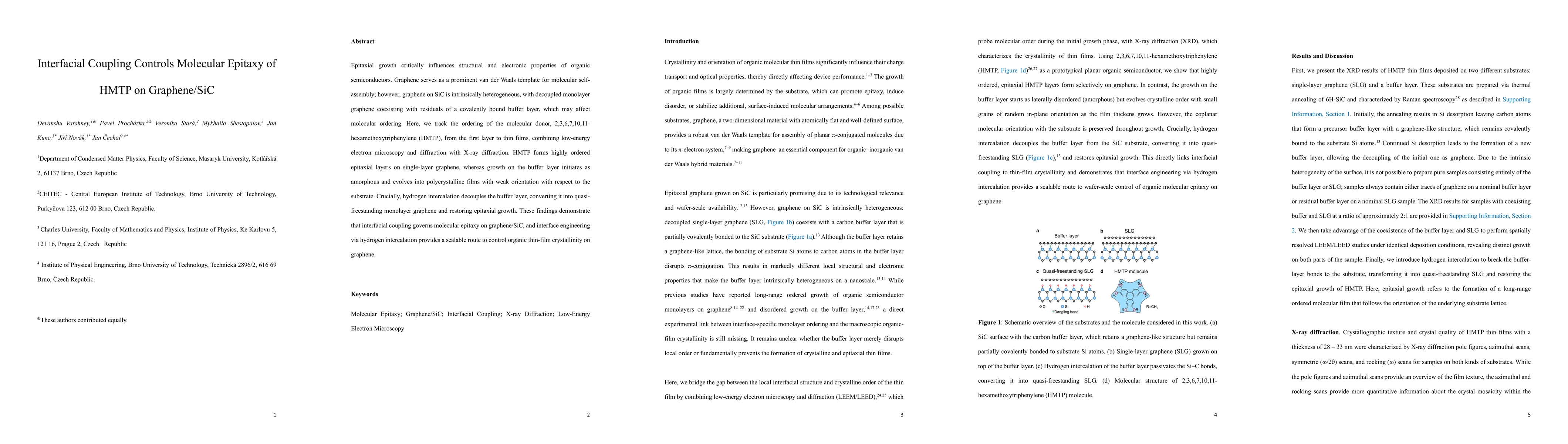
Key Findings, in focus

Seven facets of this paper, analysed and brought into focus by AI.

AI-generated · verify against source Generated Feb 02, 2026
In focus · one-line synthesis

This research provides critical insights into the growth mechanisms of 2D materials on graphene and buffer layers, which could enable the development of advanced electronic devices with precisely controlled atomic-scale structures.

01
MethodologyHow they did it

The study employed a combination of Raman spectroscopy, X-ray diffraction (XRD), atomic force microscopy (AFM), low-energy electron diffraction (LEED), and low-energy electron microscopy (LEEM) to characterize the structural and electronic properties of hexamethyldisiloxane (HMTP) films on different substrates.

02
ResultsWhat they found
  • HMTP forms a crystalline, quasi-freestanding monolayer on single-layer graphene (SLG) with a specific in-plane orientation
  • The presence of a buffer layer significantly affects HMTP crystallization, leading to less ordered domains on the buffer layer
  • LEED and LEEM analyses reveal that HMTP domains on SLG exhibit a commensurate superstructure with a 2√7 × 2√7 R19.1° unit cell
03
SignificanceWhy it matters

This research provides critical insights into the growth mechanisms of 2D materials on graphene and buffer layers, which could enable the development of advanced electronic devices with precisely controlled atomic-scale structures.

04
Technical ContributionsWhat's new technically

Development of a comprehensive characterization framework combining multiple advanced microscopy and spectroscopy techniques for studying 2D material growth

05
NoveltyWhat sets it apart

The work demonstrates how interfacial interactions between HMTP and substrates (SLG vs buffer layer) can lead to distinct crystallization behaviors, offering new strategies for controlling 2D material morphology

06
LimitationsWhat to be cautious about
  • The study primarily focuses on HMTP on specific substrates, limiting generalizability to other materials
  • The resolution of LEEM might not capture all subtle structural details
07
Future WorkWhere it goes next
  • Investigating HMTP growth on other 2D materials beyond graphene
  • Exploring the effects of different buffer layers on HMTP crystallization

Paper Details

Paper ID: 2601.22263
Categories:
cond-mat.mtrl-sci

How to Cite This Paper

Reference manager: RIS EndNote


Discussion 0

This website uses cookies to ensure you get the best experience. Learn more