Publication
Metrics
AI Quick Summary
InterMat combines density functional theory (DFT) and graph neural networks (GNN) to predict semiconductor interface band offsets, achieving high accuracy in work function, electron affinity, and band offset calculations. It employs DFT to benchmark and GNN for rapid heterojunction predictions, enabling the pre-screening of potential semiconductor devices.
Paper Preview
Abstract
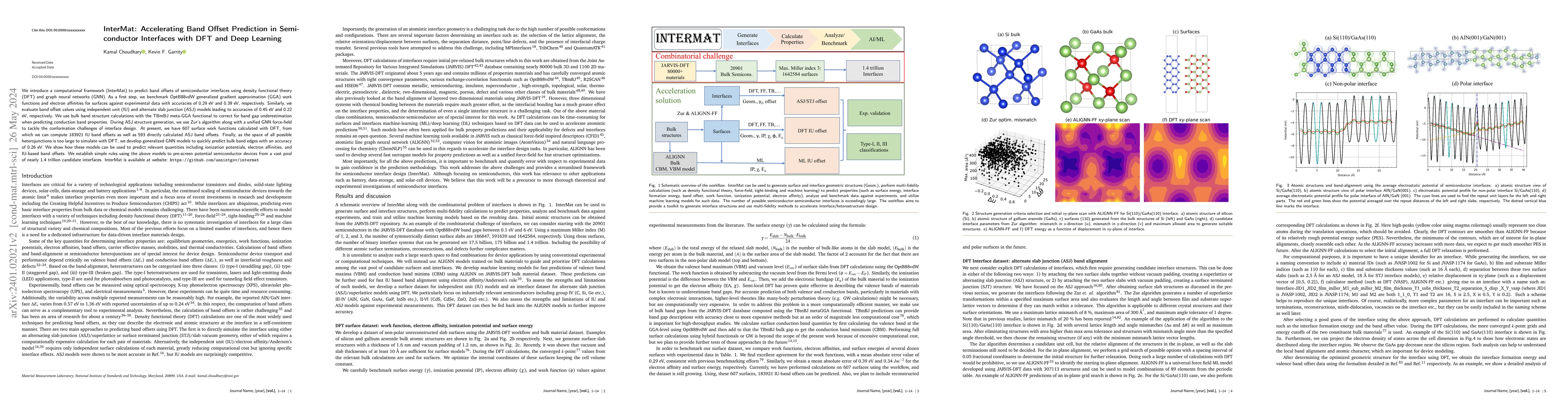
We introduce a computational framework (InterMat) to predict band offsets of semiconductor interfaces using density functional theory (DFT) and graph neural networks (GNN). As a first step, we benchmark OptB88vdW generalized gradient approximation (GGA) work functions and electron affinities for surfaces against experimental data with accuracies of 0.29 eV and 0.39 eV, respectively. Similarly, we evaluate band offset values using independent unit (IU) and alternate slab junction (ASJ) models leading to accuracies of 0.45 eV and 0.22 eV, respectively. We use bulk band structure calculations with the TBmBJ meta-GGA functional to correct for band gap underestimation when predicting conduction band properties. During ASJ structure generation, we use Zur algorithm along with a unified GNN force-field to tackle the conformation challenges of interface design. At present, we have 607 surface work functions calculated with DFT, from which we can compute 183921 IU band offsets as well as 593 directly calculated ASJ band offsets. Finally, as the space of all possible heterojunctions is too large to simulate with DFT, we develop generalized GNN models to quickly predict bulk band edges with an accuracy of 0.26 eV. We show how these models can be used to predict relevant quantities including ionization potentials, electron affinities, and IU-based band offsets. We establish simple rules using the above models to pre-screen potential semiconductor devices from a vast pool of nearly 1.4 trillion candidate interfaces. InterMat is available at website: https://github.com/usnistgov/intermat
AI Key Findings
Get AI-generated insights about this paper's methodology, results, significance, and more — seven facets brought into focus.
Impact
Paper Details
Authors
PDF Preview
Key Terms
Citation Network
Current paper (gray), citations (green), references (blue)
Display is limited for performance on very large graphs.
Discussion 0