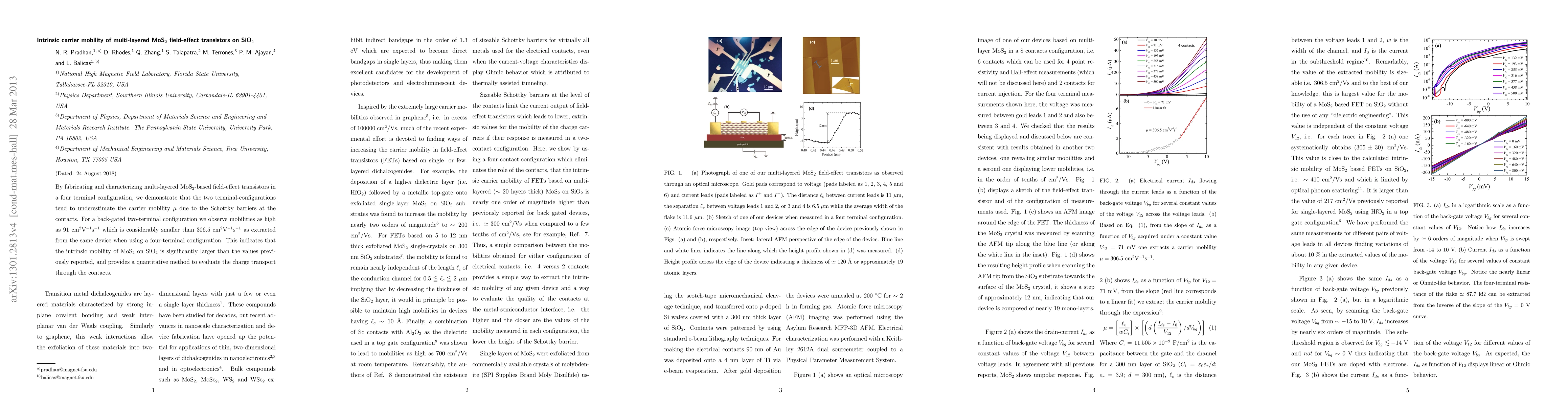
This study demonstrates that intrinsic carrier mobility in multi-layered MoS$_2$ field-effect transistors is significantly underestimated in two-terminal configurations due to Schottky barriers. Four-terminal measurements reveal intrinsic mobilities up to 306.5 cm$^2$V$^{-1}$s$^{-1}$, highlighting a substantial discrepancy from the 125 cm$^2$V$^{-1}$s$^{-1}$ observed in two-terminal setups.
By fabricating and characterizing multi-layered MoS$_2$-based field-effect transistors (FETs) in a four terminal configuration, we demonstrate that the two terminal-configurations tend to underestimate the carrier mobility $\mu$ due to the Schottky barriers at the contacts. For a back-gated two-terminal configuration we observe mobilities as high as 125 cm$^2$V$^{-1}$s$^{-1}$ which is considerably smaller than 306.5 cm$^2$V$^{-1}$s$^{-1}$ as extracted from the same device when using a four-terminal configuration. This indicates that the intrinsic mobility of MoS$_2$ on SiO$_2$ is significantly larger than the values previously reported, and provides a quantitative method to evaluate the charge transport through the contacts.
This graph shows how this paper is connected to other research. The current paper is shown in dark gray, papers that cite it are in green, and papers it references are in blue. You can:
• Hover over any node to see the paper title
• Click a node to view that paper's details
• Drag nodes to rearrange the graph
• Use the zoom controls (bottom right) to zoom in/out
Title | Authors | Year | Actions |
---|---|---|---|
High carrier mobility and strong anisotropy in the family of monolayer SnP2X6 (X=S, Se, Te)
|
Feng Li, Xiangyan Bo, Chenglong Wu, Yang Zhang, Shasha Li, Hong Wu
|
2024
|
View Paper |
Structural and photoluminescence properties of terbium (III) activated Li2SiO3 phosphors: an approach for bluish-green light emission
|
Priya Barik, Aksh Kumar Verma, Ravinder Kumar, Vinod Kumar, P. Dewangan, Manorama Sahu, I. P. Sahu
|
2024
|
View Paper |
Electronic and optical properties of Zr2CO2/WS2 van der Waals heterostructures: First-principles study
|
Rui Zhou, Hua Tong, Qingguo Xu, Guoqiang Hao, Ruidong Zhang
|
2024
|
View Paper |
Spreading resistance and conductance anisotropy in multilayer MoS2
|
Gautham Vijayan, Michael Uzhansky, E. Koren
|
2024
|
View Paper |
Tensile Strain Induced Anomalous Enhancement in the Lattice Thermal Transport of Monolayer ZnO: A First Principles Study
|
S. Chaudhuri, Amrita Bhattacharya, A. K. Das, G. P. Das, B. N. Dev
|
2023
|
View Paper |
Physical vapor deposition-free scalable high-efficiency electrical contacts to MoS2
|
Anusha Shanmugam, Muhammad Arshad Thekke Purayil, Sai Abhishikth Dhurjati, M. Thalakulam
|
2023
|
View Paper |
Phase Engineering of Two‐Dimensional Transition Metal Dichalcogenides
|
Jong Hun Kim, Hayeong Sung, Gwan‐Hyoung Lee
|
2023
|
View Paper |
Vinyl-Flanked Diketopyrrolopyrrole Polymer/MoS2 Hybrid for Donor–Acceptor Semiconductor Photodetection
|
Ranganath Wahalathantrige Don, Priyanka Das, Ziyuan Ma, Udara M. Kuruppu, Da-Fa Feng, B. Shook, Mahesh K. Gangishetty, M. Stefan, N. Pradhan, Colleen N. Scott
|
2023
|
View Paper |
Ab Initio Study of Electronic and Lattice Dynamical Properties of Monolayer ZnO Under Strain
|
S. Chaudhuri, A. K. Das, G. P. Das, B. Dev
|
2022
|
View Paper |
Strain Induced Effects on the Electronic and Phononic Properties of 2h and 1t ′ Monolayer Mos 2
|
S. Chaudhuri, A. Das, G. P. Das, B. N. Dev
|
2022
|
View Paper |
Origin of phonon-limited mobility in two-dimensional metal dichalcogenides
|
Hao Chang, Hao Wang, Keke Song, Min Zhong, Li-Bin Shi, P. Qian
|
2021
|
View Paper |
Achievement of strain-driven ultrahigh carrier mobility in β-TeO2
|
R. K. Biswas, S. Pati
|
2021
|
View Paper |
Origin of low-temperature negative transconductance in multilayer MoS2 transistors
|
Qi Chen, Guoli Li, Yuan Liu, N. André, Xingqiang Liu, Z. Xia, D. Flandre, L. Liao
|
2021
|
View Paper |
Determination of interlayer electron mobility in multilayer MoS2 flake using impedance spectroscopy
|
S. Srivastava, Y. N. Mohapatra
|
2021
|
View Paper |
Air-stable and efficient electron doping of monolayer MoS2 by salt-crown ether treatment.
|
Hiroto Ogura, M. Kaneda, Y. Nakanishi, Y. Nonoguchi, J. Pu, M. Ohfuchi, T. Irisawa, HongEn Lim, T. Endo, K. Yanagi, T. Takenobu, Y. Miyata
|
2021
|
View Paper |
Dramatic Reduction of Contact Resistance via Ultrathin LiF in Two-Dimensional MoS2 Field Effect Transistors.
|
Hyunmin Cho, Donghee Kang, Yangjin Lee, Heesun Bae, Sungjae Hong, Yongjae Cho, Kwanpyo Kim, Y. Yi, Ji Hoon Park, S. Im
|
2021
|
View Paper |
Peroxide-Induced Tuning of the Conductivity of Nanometer-Thick MoS2 Films for Solid-State Sensors
|
D. Saha, P. Selvaganapathy, P. Kruse
|
2020
|
View Paper |
High broadband photoconductivity of few-layered MoS2 field-effect transistors measured using multi-terminal methods: effects of contact resistance.
|
Priyanka Das, J. Nash, M. Webb, R. Burns, V. Mapara, Govinda Ghimire, D. Rosenmann, R. Divan, D. Karaiskaj, S. McGill, A. Sumant, Qilin Dai, P. Ray, Bhausaheb V. Tawade, D. Raghavan, A. Karim, N. Pradhan
|
2020
|
View Paper |
Device Architecture for Visible and Near-Infrared Photodetectors Based on Two-Dimensional SnSe2 and MoS2: A Review
|
E. P. Mukhokosi, G. V. S. Manohar, T. Nagao, S. .. Krupanidhi, K. Nanda
|
2020
|
View Paper |
Intrinsic Photoconductivity of few-layered ZrS2 Phototransistors via Multiterminal Measurements
|
Rukshan M. Tanthirige, C. García, Saikat Ghosh, F. Jackson, J. Nash, D. Rosenmann, R. Divan, L. Stan, A. Sumant, S. McGill, P. Ray, N. Pradhan
|
2020
|
View Paper |
Controlled polymer crystal/two-dimensional material heterostructures for high-performance photoelectronic applications.
|
Kang Lib Kim, Min Koo, Cheolmin Park
|
2020
|
View Paper |
Accurate Method To Determine the Mobility of Transition-Metal Dichalcogenides with Incomplete Gate Screening.
|
R. Dagan, Y. Vaknin, Dror Weisman, I. Amit, Y. Rosenwaks
|
2019
|
View Paper |
Low-temperature behaviors of multilayer MoS2 transistors with ohmic and Schottky contacts
|
Woong Choi, Demin Yin, Sooho Choo, S. Jeong, Hyuk‐Jun Kwon, Y. Yoon, Sunkook Kim
|
2019
|
View Paper |
A multi-level bipolar memristive device based on visible light sensing MoS2 thin film
|
Ujjal Das, S. Bhattacharjee, P. Sarkar, A. Roy
|
2019
|
View Paper |
Universal Fermi-Level Pinning in Transition-Metal Dichalcogenides
|
K. Sotthewes, R. van Bremen, E. Dollekamp, T. Boulogne, Krystian Nowakowski, Daan Kas, H. Zandvliet, P. Bampoulis
|
2019
|
View Paper |
Transition metal dichalcogenides bilayer single crystals by reverse-flow chemical vapor epitaxy
|
Xiumei Zhang, H. Nan, S. Xiao, Xi Wan, Xiaofeng Gu, A. Du, Zhenhua Ni, K. Ostrikov
|
2019
|
View Paper |
Photogating and high gain in ReS2 field-effect transistors
|
C. García, N. Pradhan, D. Rhodes, L. Balicas, S. McGill
|
2018
|
View Paper |
Experimentally Measured Field Effect Mobilities for Few Layer van der Waals Materials
|
S. Sylvia, R. Lake
|
2018
|
View Paper |
Elastic Scattering of Mo-Mo, Mo-S and S-S Atomic Pairs in the Relative Kinetic Energy Range of 2–200 eV
|
A. Palov
|
2018
|
View Paper |
Resistivity of nano-devices based on MoS2 in low temperature
|
Z. Tao, H. Dong, F. Huang, J. L. Liu
|
2018
|
View Paper |
Analysis of optical and electronic properties of MoS2 for optoelectronics and FET applications
|
M. S. Ullah, A. H. Yousuf, Azzedin D. Es-Sakhi, M. Chowdhury
|
2018
|
View Paper |
Effects of H2O2 treatment on the temperature-dependent behavior of carrier transport and the optoelectronic properties for sol–gel grown MoS2/Si nanowire/Si devices
|
C. Wu, Y. Lin, Hsing-Cheng Chang, Ya-Hui Chen
|
2018
|
View Paper |
Temperature dependence of current-voltage characteristics of MoS2/Si devices prepared by the chemical vapor deposition method
|
T. Su, C. Chiang, Y. Lin
|
2017
|
View Paper |
Highly Enhanced H2 Sensing Performance of Few-Layer MoS2/SiO2/Si Heterojunctions by Surface Decoration of Pd Nanoparticles
|
L. Hao, Yunjie Liu, Yongjun Du, Zhaoyang Chen, Zhide Han, Zhijie Xu, Jun Zhu
|
2017
|
View Paper |
Fabrication and electrical performance of CVD-grown MoS2 transistor
|
Ming Wen, Jiqu Xu, L. Liu, Xinyuan Zhao, P. T. Lai, W. Tang
|
2017
|
View Paper |
Behavior of carrier transports and their sensitivity to solar irradiation for devices that use MoS2 that is directly deposited on Si using the chemical vapor method
|
Y. Lin, T. Su, S. Chen
|
2017
|
View Paper |
Sensitive optical bio-sensing of p-type WSe2 hybridized with fluorescent dye attached DNA by doping and de-doping effects
|
K. Han, Jun Young Kim, S. Jo, Changwon Seo, Jeongyong Kim, J. Joo
|
2017
|
View Paper |
Using Imperfect Semiconductor Systems for Unique Identification
|
J. Roberts
|
2017
|
View Paper |
Transport properties and device-design of Z-shaped MoS 2 nanoribbon planar junctions
|
Hua Zhang, Wenzhe Zhou, Qi Liu, Zhixiong Yang, Jiangling Pan, Fangping Ouyang, Hui Xu
|
2017
|
View Paper |
Responsivity to solar irradiation and the behavior of carrier transports for MoS2/Si and MoS2/Si nanowires/Si devices
|
C. Wu, Y. Lin
|
2017
|
View Paper |
Layered material GeSe and vertical GeSe/MoS2 p-n heterojunctions
|
W. C. Yap, Zhengfeng Yang, Mehrshad Mehboudi, Jia-An Yan, S. Barraza‐Lopez, Wenjuan Zhu
|
2017
|
View Paper |
Hysteresis in the transfer characteristics of MoS2 transistors
|
A. Di Bartolomeo, L. Genovese, F. Giubileo, L. Iemmo, G. Luongo, Tobias Foller, M. Schleberger
|
2017
|
View Paper |
Electron transport in some transition metal di-chalcogenides: MoS2 and WS2
|
D. Ferry
|
2017
|
View Paper |
Controlling the electronic and geometric structures of 2D insertions to realize high performance metal/insertion-MoS2 sandwich interfaces.
|
J. Su, Li-ping Feng, Wei Zeng, Zheng-tang Liu
|
2017
|
View Paper |
Recent Advances in Electronic and Optoelectronic Devices Based on Two-Dimensional Transition Metal Dichalcogenides
|
Mingxiao Ye, Dongyang Zhang, Y. Yap
|
2017
|
View Paper |
Surface Plasmon Resonance Effect of the MoS2/Ag System
|
X. Ma, Hongmin Mao, Miaofei Meng
|
2017
|
View Paper |
Optoelectronic Properties of Heterostructures: The Most Recent Developments Based on Graphene and Transition-Metal Dichalcogenides
|
N. Pradhan, S. Talapatra, M. Terrones, P. Ajayan, L. Balicas
|
2017
|
View Paper |
SiO2 substrate passivation effects on the temperature-dependent electrical properties of MoS2 prepared by the chemical vapor deposition method
|
Y. Lin, T. Su
|
2017
|
View Paper |
A Facile Synthesis and Photoluminescence Properties of SiO 2 :Tb 3+ Spherical Nanoparticles
|
Murad M. A. Abualrejal, H. Zou, Jie Chen, Yanhua Song, Ye Sheng
|
2017
|
View Paper |
Performance Investigation of Multilayer MoS2 Thin-Film Transistors Fabricated via Mask-free Optically Induced Electrodeposition.
|
Meng Li, Na Liu, Pan Li, Jialin Shi, Guangyong Li, N. Xi, Yuechao Wang, Lianqing Liu
|
2017
|
View Paper |
Vacuum ultraviolet radiation effects on two-dimensional MoS2 field-effect transistors
|
J. McMorrow, C. Cress, Heather N. Arnold, V. Sangwan, D. Jariwala, S. Schmucker, T. Marks, M. Hersam
|
2017
|
View Paper |
Chemical vapor deposition of monolayer MoS2 directly on ultrathin Al2O3 for low-power electronics
|
Hadallia Bergeron, V. Sangwan, J. McMorrow, Gavin P. Campbell, Itamar Balla, Xiaolong Liu, M. Bedzyk, T. Marks, M. Hersam
|
2017
|
View Paper |
MoS2 based dual input logic AND gate
|
Luis M. Martinez, N. Pinto, Carl H. Naylor, A. T. Johnson
|
2016
|
View Paper |
Engineering the optoelectronic properties of MoS2 photodetectors through reversible noncovalent functionalization.
|
A. Molina‐Mendoza, Luis Vaquero-Garzon, Sofía Leret, Leire de Juan-Fernández, E. Pérez, A. Castellanos-Gomez
|
2016
|
View Paper |
Photoconductivity of few-layered p-WSe2 phototransistors via multi-terminal measurements
|
N. Pradhan, C. García, Joshua Holleman, D. Rhodes, Chason Parker, S. Talapatra, M. Terrones, L. Balicas, S. McGill
|
2016
|
View Paper |
Electron velocity saturation and intervalley transfer in monolayer MoS2
|
D. Ferry
|
2016
|
View Paper |
Two- and four-probe field-effect and Hall mobilities in transition metal dichalcogenide field-effect transistors
|
Ghazanfar Nazir, Muhammad Farooq Khan, V. M. Iermolenko, J. Eom
|
2016
|
View Paper |
Atomistic modeling of the metallic-to-semiconducting phase boundaries in monolayer MoS2
|
D. Saha, S. Mahapatra
|
2016
|
View Paper |
Study of the surface plasmon properties in MoS2–Ag film system
|
ShiWeilin, ShiMiaoyuan, MaXiying
|
2016
|
View Paper |
Thickness dependence of surface energy and contact angle of water droplets on ultrathin MoS2 films.
|
Yanhua Guo, Zhengfei Wang, Lizhi Zhang, Xiaodong Shen, Feng Liu
|
2016
|
View Paper |
Photoluminescence profiles and fast/slow annealing effects of Eu(III)/Tb(III)-codoped silica phosphor materials.
|
H. Yoon, Y. Choi, Jun-Gill Kang, Y. Sohn
|
2016
|
View Paper |
Immunity of electronic and transport properties of phosphorene nanoribbons to edge defects
|
M. Poljak, T. Suligoj
|
2016
|
View Paper |
Theoretical analysis of the combined effects of sulfur vacancies and analyte adsorption on the electronic properties of single-layer MoS2
|
B. Akdim, R. Pachter, S. Mou
|
2016
|
View Paper |
Charge transport and mobility engineering in two-dimensional transition metal chalcogenide semiconductors.
|
Songlin Li, K. Tsukagoshi, E. Orgiu, P. Samorí
|
2016
|
View Paper |
3D Behavior of Schottky Barriers of 2D Transition-Metal Dichalcogenides.
|
Yuzheng Guo, Dameng Liu, J. Robertson
|
2015
|
View Paper |
Scalable fabrication of a hybrid field-effect and acousto-electric device by direct growth of monolayer MoS2/LiNbO3
|
E. Preciado, F. J. Schülein, A. Nguyen, David Barroso, Miguel Isarraraz, Gretel von Son, I. Lu, W. Michailow, B. Möller, V. Klee, J. Mann, A. Wixforth, L. Bartels, H. Krenner
|
2015
|
View Paper |
Surface confined quantum well state in MoS2(0001) thin film
|
Jiatao Sun, S. Song, S. Meng, S. Du, Feng Liu, H. J. Gao
|
2015
|
View Paper |
Visibility of two-dimensional layered materials on various substrates
|
M. Muller, A. Gumprich, E. Eçik, K. Kallis, F. Winkler, B. Kardynał, I. Petrov, U. Kunze, J. Knoch
|
2015
|
View Paper |
Metal to Insulator Quantum-Phase Transition in Few-Layered ReS₂.
|
N. Pradhan, A. McCreary, D. Rhodes, Zhengguang Lu, S. Feng, E. Manousakis, D. Smirnov, R. Namburu, M. Dubey, A. Walker, H. Terrones, M. Terrones, V. Dobrosavljević, L. Balicas
|
2015
|
View Paper |
Two-dimensional transition metal dichalcogenides: Clusters, ribbons, sheets and more
|
R. Lv, H. Terrones, A. Elías, N. Peréa-López, H. Gutiérrez, E. Cruz‐Silva, L. P. Rajukumar, M. Dresselhaus, M. Terrones
|
2015
|
View Paper |
Bulk transport and contact limitation of MoS2 multilayer flake transistors untangled via temperature‐dependent transport measurements
|
I. Vladimirov, C. Chow, A. Strudwick, W. Kowalsky, M. Schwab, D. Kälblein, R. Weitz
|
2015
|
View Paper |
A Theoretical Investigation of Orientation-Dependent Transport in Monolayer MoS2 Transistors at the Ballistic Limit
|
Fei Liu, Yijiao Wang, Xiaoyan Liu, Jian Wang, Hong Guo
|
2015
|
View Paper |
Comparative Study on Electronic Structures of Sc and Ti Contacts with Monolayer and Multilayer MoS2.
|
Zhongjun Li, Xingxing Li, Jinlong Yang
|
2015
|
View Paper |
High Photoresponsivity and Short Photoresponse Times in Few-Layered WSe2 Transistors.
|
N. Pradhan, J. Ludwig, Zhengguang Lu, D. Rhodes, Michael Bishop, K. Thirunavukkuarasu, S. McGill, D. Smirnov, L. Balicas
|
2015
|
View Paper |
Facile fabrication of a ultraviolet tunable MoS2/p-Si junction diode
|
W. Serrano, N. Pinto, Carl H. Naylor, N. Kybert, A. T. Johnson
|
2015
|
View Paper |
Chalcogen vacancies in monolayer transition metal dichalcogenides and Fermi level pinning at contacts
|
Yuzheng Guo, Dameng Liu, J. Robertson
|
2015
|
View Paper |
Modeling accumulation capacitance-voltage characteristic of MoS2 thin flake transistors
|
Boping Hu
|
2015
|
View Paper |
Electrochemical synthesis of luminescent MoS2 quantum dots.
|
D. Gopalakrishnan, Dijo Damien, Bo Li, Hemtej Gullappalli, V. Pillai, P. Ajayan, M. Shaijumon
|
2015
|
View Paper |
Fabrication of high-k/metal-gate MoS2 field-effect transistor by device isolation process utilizing Ar-plasma etching
|
N. Ninomiya, T. Mori, N. Uchida, E. Watanabe, D. Tsuya, S. Moriyama, Masatoshi Tanaka, A. Ando
|
2015
|
View Paper |
Advances in MoS2-Based Field Effect Transistors (FETs)
|
X. Tong, E. Ashalley, Feng Lin, Handong Li, Zhiming M. Wang
|
2015
|
View Paper |
Hall and field-effect mobilities in few layered p-WSe2 field-effect transistors
|
N. Pradhan, D. Rhodes, S. Memaran, J. Poumirol, D. Smirnov, S. Talapatra, S. Feng, N. Peréa-López, A. Elías, M. Terrones, P. Ajayan, L. Balicas
|
2015
|
View Paper |
Large variations in both dark- and photoconductivity in nanosheet networks as nanomaterial is varied from MoS2 to WTe2.
|
G. Cunningham, D. Hanlon, N. McEvoy, G. Duesberg, J. Coleman
|
2015
|
View Paper |
Variability of electrical contact properties in multilayer MoS2 thin-film transistors
|
S. Kim, Seonyoung Park, Woong Choi
|
2014
|
View Paper |
Hot-electron cooling by acoustic and optical phonons in monolayers of MoS 2 and other transition-metal dichalcogenides
|
K. Kaasbjerg, K. Bhargavi, S. Kubakaddi
|
2014
|
View Paper |
High intrinsic mobility and ultrafast carrier dynamics in multilayer metal-dichalcogenideMoS2
|
J. Strait, P. Nene, F. Rana
|
2014
|
View Paper |
Ambipolar molybdenum diselenide field-effect transistors: field-effect and Hall mobilities.
|
N. Pradhan, D. Rhodes, Y. Xin, S. Memaran, L. Bhaskaran, M. Siddiq, S. Hill, P. Ajayan, L. Balicas
|
2014
|
View Paper |
Field-effect transistors based on few-layered α-MoTe(2).
|
N. Pradhan, D. Rhodes, S. Feng, Y. Xin, S. Memaran, B. Moon, H. Terrones, M. Terrones, L. Balicas
|
2014
|
View Paper |
CVD-grown monolayered MoS2 as an effective photosensor operating at low-voltage
|
N. Peréa-López, Zhong Lin, N. Pradhan, A. Iniguez-Rabago, Ana Laura Elias, A. McCreary, J. Lou, P. Ajayan, H. Terrones, L. Balicas, M. Terrones
|
2014
|
View Paper |
Density Functional Theory Study of Chemical Sensing on Surfaces of Single-Layer MOS2 and Graphene (Postprint)
|
F. Mehmood, R. Pachter
|
2014
|
View Paper |
Fabrication and electrical properties of MoS2 nanodisc-based back-gated field effect transistors
|
Weixia Gu, J. Shen, Xiying Ma
|
2014
|
View Paper |
Emerging device applications for semiconducting two-dimensional transition metal dichalcogenides.
|
D. Jariwala, V. Sangwan, L. Lauhon, T. Marks, M. Hersam
|
2014
|
View Paper |
IMPROVEMENT IN MOBILITY AND CONDUCTIVITY OF FEW-LAYER MoS2 FILMS
|
Xiying Ma, Jie He, Kangye Chen, La Lin
|
2014
|
View Paper |
Electronic transport and device prospects of monolayer molybdenum disulphide grown by chemical vapour deposition
|
Wenjuan Zhu, T. Low, Yi‐Hsien Lee, Han Wang, D. Farmer, J. Kong, F. Xia, P. Avouris
|
2014
|
View Paper |
Role of strain on electronic and mechanical response of semiconducting transition-metal dichalcogenide monolayers: An ab-initio study
|
D. Guzman, A. Strachan
|
2013
|
View Paper |
Sulfur vacancies in monolayer MoS2 and its electrical contacts
|
Dameng Liu, Yuzheng Guo, L. Fang, J. Robertson
|
2013
|
View Paper |
Magneto-transport in MoS2: phase coherence, spin-orbit scattering, and the hall factor.
|
A. Neal, Han Liu, J. Gu, P. Ye
|
2013
|
View Paper |
Thermal Evaporation Deposition of Few-layer MoS2 Films
|
Xiying Ma, Miaoyuan Shi
|
2013
|
View Paper |
Recent Progress in Ferroelectric Diodes: Explorations in Switchable Diode Effect
|
C. Ge, Can Wang, K. Jin, Hui‐bin Lu, Guo‐zhen Yang
|
2013
|
View Paper |
Band-like transport in high mobility unencapsulated single-layer MoS 2 transistors
|
D. Jariwala, V. Sangwan, D. Late, J. Johns, V. Dravid, T. Marks, L. Lauhon, M. Hersam
|
2013
|
View Paper |
Progress, challenges, and opportunities in two-dimensional materials beyond graphene.
|
Sheneve Butler, S. Hollen, Linyou Cao, Yi Cui, J. Gupta, H. Gutiérrez, T. Heinz, S. Hong, Jiaxing Huang, A. Ismach, E. Johnston-Halperin, M. Kuno, Vladimir V. Plashnitsa, R. D. Robinson, R. Ruoff, S. Salahuddin, J. Shan, Li Shi, M. Spencer, M. Terrones, W. Windl, J. Goldberger
|
2013
|
View Paper |
Large Area Single Crystal (0001) Oriented MoS2 Thin Films
|
M. Laskar, Lu Ma, S. Kannappan, P. Park, S. Krishnamoorthy, D. Nath, W. Lu, Yiying Wu, S. Rajan
|
2013
|
View Paper |
Interlayer angle-dependent electronic structure and optoelectronic properties of BP-MoS2 heterostructure: A first principle study
|
Innocent Joseph, Kaiwei Wan, S. Hussain, Lingju Guo, Liming Xie, Xinghua Shi
|
2021
|
View Paper |
Nonreciprocal absorption and omnidirectional band gap in the biaxial hyperbolic metamaterials with black phosphorus
|
Yu Ma, Mingyu Mao, Hai‐feng Zhang
|
2021
|
View Paper |
Electronic and optoelectronic properties of the heterostructure devices composed of two-dimensional layered materials
|
N. Pradhan, R. Thantirige, Prasanna D. Patil, S. McGill, S. Talapatra
|
2020
|
View Paper |
Voltage-Controlled Deposition of Nanoparticles for Next Generation Electronic Materials
|
S. Maulik
|
2018
|
View Paper |
Controlled growth of MoS 2 nanopetals on the silicon nanowire array using the chemical vapor deposition method
|
S. Chen, Y. Lin
|
2018
|
View Paper |
Electrical and optoelectronic properties for devices that use MoS2 deposited on Si substrates with and without (NH4)2Sx treatment by chemical vapor deposition
|
T. Su, Chang-Lin Wu, Hsing-Cheng Chang, Y. Lin
|
2017
|
View Paper |
Langmuir-Blodgett Deposition of 2D Materials for Unique Identification
|
J. Roberts
|
2017
|
View Paper |
Investigation of Interconnect and Device Designs for Emerging Post-MOSFET and Beyond Silicon Technologies
|
M. S. Ullah
|
2016
|
View Paper |
Emerging Applications of 2D TMDCs
|
A. Kolobov, J. Tominaga
|
2016
|
View Paper |
Structure and Physico-Chemical Properties of Single Layer and Few-Layer TMDCs
|
A. Kolobov, J. Tominaga
|
2016
|
View Paper |
Novel two-dimensional nanomaterials and their gas sensing properties
|
H. Pu
|
2015
|
View Paper |
Electronic transport in atomically thin layered materials
|
B. Baugher
|
2014
|
View Paper |
Published: 2015-03-12
Marika Schleberger, Stephan Sleziona, Osamah Kharsah, Aniello Pelella, Enver Faella, Lucia Skopinski, Andre Maas, Yossarian Liebsch, Antonio Di Bartolomeo
Published: 2023-06-08
Anjan K. Gupta, Santu Prasad Jana, Shivangi, Suraina Gupta
Published: 2024-03-12
Comments (0)