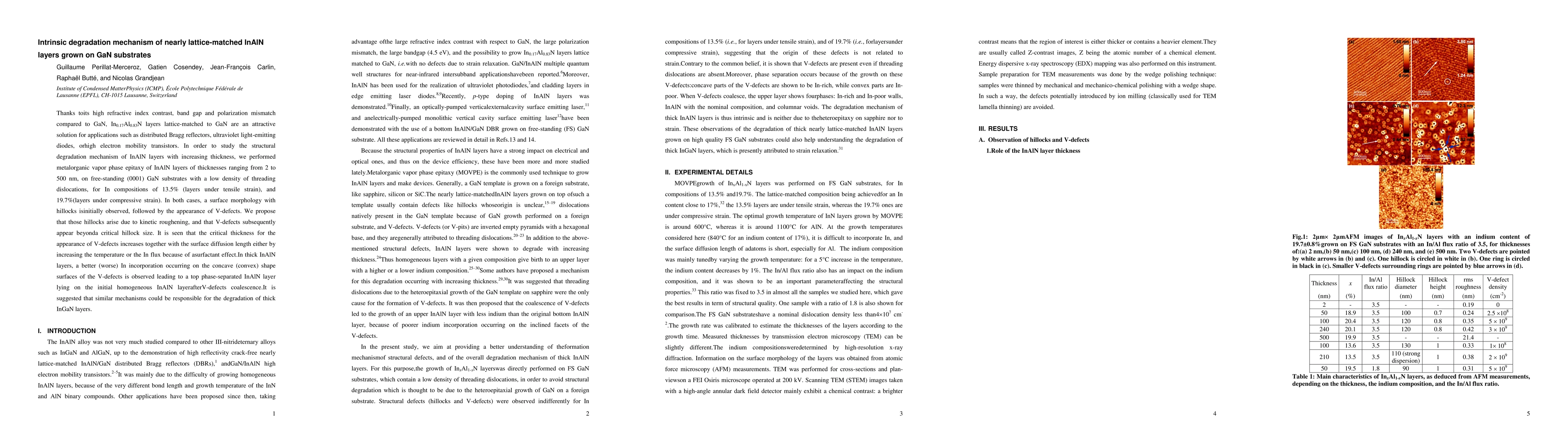
ArxivLens

Quick Summary:

This study investigates the intrinsic degradation mechanism of nearly lattice-matched InAlN layers grown on GaN substrates, revealing that hillocks and V-defects form due to kinetic roughening and surface diffusion, respectively. The critical thickness for V-defects increases with higher temperature or In flux, leading to phase separation in thick layers.

Journal Reference: Applied Physics Letters 113, 6 (2013) 063506
DOI: 10.1063/1.4790424
arXiv Id: 1302.3139
Date Published: 2013-02-14
Date Updated: 2013-02-14

Categories:

Key Terms (TF-IDF):

defects (0.283)
layers (0.268)
gan (0.256)
degradation (0.205)
strain (0.186)
thickness (0.185)
appearance (0.178)
layer (0.138)
increasing (0.136)
refractive (0.126)
compressive (0.123)
band gap (0.123)
substrates (0.122)
low density (0.122)
critical (0.121)
surface (0.121)
matched (0.119)
occurring (0.116)
lying (0.115)
emitting (0.114)
License: http://arxiv.org/licenses/nonexclusive-distrib/1.0/

Summary:

Thanks to its high refractive index contrast, band gap and polarization mismatch compared to GaN, In0.17Al0.83N layers lattice-matched to GaN are an attractive solution for applications such as distributed Bragg reflectors, ultraviolet light-emitting diodes, or high electron mobility transistors. In order to study the structural degradation mechanism of InAlN layers with increasing thickness, we performed metalorganic vapor phase epitaxy of InAlN layers of thicknesses ranging from 2 to 500 nm, on free-standing (0001) GaN substrates with a low density of threading dislocations, for In compositions of 13.5% (layers under tensile strain), and 19.7% (layers under compressive strain). In both cases, a surface morphology with hillocks is initially observed, followed by the appearance of V-defects. We propose that those hillocks arise due to kinetic roughening, and that V-defects subsequently appear beyond a critical hillock size. It is seen that the critical thickness for the appearance of V-defects increases together with the surface diffusion length either by increasing the temperature or the In flux because of a surfactant effect. In thick InAlN layers, a better (worse) In incorporation occurring on the concave (convex) shape surfaces of the V-defects is observed leading to a top phase-separated InAlN layer lying on the initial homogeneous InAlN layer after V-defects coalescence. It is suggested that similar mechanisms could be responsible for the degradation of thick InGaN layers.

Citation & Reference Network Visualization

This graph shows how this paper is connected to other research. The current paper is shown in dark gray, papers that cite it are in green, and papers it references are in blue. You can:

Current Paper
Papers citing this work (Citations)
Papers cited by this work (References)

• Hover over any node to see the paper title

• Click a node to view that paper's details

• Drag nodes to rearrange the graph

• Use the zoom controls (bottom right) to zoom in/out

Citations and References

Title Authors Year Actions
Improved surface morphology and reduced V-pits density of lattice-matched AlInN films grown by atmospheric pressure metalorganic chemical vapor deposition
Shaosheng Fan, Masao Ikeda, Baoping Zhang, Zenglin Li, Xujun Su, Zongliang Liu, Ke Xu
2024
View Paper
Advances in Room Temperature of Indium Aluminum Nitride InAlN Deposition via Direct Current (DC) Co-Sputtering for Solar Energy Applications
Juan David Cañón-Bermúdez, L. F. Mulcué-Nieto
2024
View Paper
Characterizations of Subbandgap Optical Absorption in Undoped‐GaN and 90 nm‐Thick Al1−xInxN Thin Film on Sapphire Substrates Grown by Metal–Organic Chemical Vapor Deposition
Kouki Noda, Y. Murakami, H. Toyoda, K. Shibata, Youna Tsukada, D. Imai, Tetsuya Takeuchi, Makoto Miyoshi, Takao Miyajima
2024
View Paper
InAlN cladding implementation in green superluminescent diodes and lasers
M. Malinverni, A. Castiglia, M. Rossetti, A. Ferhatovic, D. Martin, M. Duelk, C. Velez
2023
View Paper
Composition Inhomogeneity in Nonpolar (101̅0) and Semipolar (202̅1) InAlN Layers Grown by Plasma-Assisted Molecular Beam Epitaxy
M. Sawicka, J. Smalc-Koziorowska, Marcin Kryśko, Natalia Fiuczek, P. Wolny, A. Feduniewicz-Żmuda, K. Nowakowski-Szkudlarek, H. Turski, C. Skierbiszewski
2021
View Paper
Lattice-matched III-nitride structures comprising BAlN, BGaN, and AlGaN for ultraviolet applications
F. AlQatari, M. Sajjad, Ronghui Lin, Kuang-Hui Li, U. Schwingenschlögl, Xiaohang Li
2021
View Paper
Challenges and Advancement of Blue III-Nitride Vertical-Cavity Surface-Emitting Lasers
Chia-Yen Huang, K. Hong, Zhen‐Ting Huang, Wen-Hsuan Hsieh, Wei-Hao Huang, T. Lu
2021
View Paper
Growth of 300-nm-thick epitaxial AlInN films on a semi-relaxed c-plane GaInN template by metalorganic chemical vapor deposition
M. Miyoshi, M. Yamanaka, T. Egawa, N. Okada, K. Tadatomo, T. Takeuchi
2021
View Paper
Low-resistivity vertical current transport across AlInN/GaN interfaces
P. Sana, C. Seneza, C. Berger, H. Witte, M. Schmidt, J. Bläsing, S. Neugebauer, Florian Hoerich, A. Dadgar, A. Strittmatter
2020
View Paper
Indium segregation mechanism and V-defect formation at the [0001] InAlN surface: an ab-initio investigation
R. Mohamad, P. Ruterana
2020
View Paper
Low background doping in AlInN grown on GaN via metalorganic vapor phase epitaxy
D. Borovac, Wei‐Che Sun, Matthew R. Peart, Renbo Song, Jonathan J. Wierer, N. Tansu
2020
View Paper
Polariton relaxation and polariton nonlinearities in nonresonantly cw-pumped III-nitride slab waveguides
J. Ciers, D. Solnyshkov, G. Callsen, Y. Kuang, J. Carlin, G. Malpuech, R. Butté, N. Grandjean
2020
View Paper
Role of high nitrogen flux in InAlN growth by plasma-assisted molecular beam epitaxy
M. Sawicka, Natalia Fiuczek, P. Wolny, A. Feduniewicz-Żmuda, M. Siekacz, Marcin Kryśko, K. Nowakowski-Szkudlarek, J. Smalc-Koziorowska, S. Kret, Ž. Gačević, E. Calleja, C. Skierbiszewski
2020
View Paper
On the thermal stability of nearly lattice-matched AlInN films grown on GaN via MOVPE
D. Borovac, Wei‐Che Sun, Renbo Song, Jonathan J. Wierer, N. Tansu
2020
View Paper
Growth evolution of N-polar indium-rich InAlN layer on c-sapphire via strain relaxation by ultrathin AlON interlayer
P. Chauhan, S. Hasenöhrl, A. Minj, M. Chauvat, P. Ruterana, J. Kuzmík
2020
View Paper
The effect of N-vacancy and In aggregation on the properties of InAlN
R. Mohamad, Jun Chen, P. Ruterana
2020
View Paper
InxAl1 –xN Solid Solutions: Composition Stability Issues
V. Brudnyi, M. D. Vilisova, L. E. Velikovskiy
2019
View Paper
The critical role of N-vacancy on chemical composition fluctuations and degradation of InAlN layer
R. Mohamad, M. Chauvat, S. Kret, P. Gamarra, S. Delage, Viwanou Hounkpati, C. Lacam, Jun Chen, P. Ruterana
2019
View Paper
V-pit pinning at the interface of high and low-temperature gallium nitride growth
R. Bouveyron, M. Mrad, M. Charles
2019
View Paper
Microscopic analysis of interface composition dynamics in m-plane AlInN
P. Horenburg, H. Bremers, R. Imlau, U. Rossow, A. Hangleiter
2019
View Paper
A 300 nm thick epitaxial AlInN film with a highly flat surface grown almost perfectly lattice-matched to c-plane free-standing GaN substrate
M. Miyoshi, M. Yamanaka, T. Egawa, T. Takeuchi
2019
View Paper
Evidence of relationship between strain and In-incorporation: Growth of N-polar In-rich InAlN buffer layer by OMCVD
P. Chauhan, S. Hasenöhrl, E. Dobročka, M. Chauvat, A. Minj, F. Gucmann, Ľ. Vančo, J. Kováč, S. Kret, P. Ruterana, Martin Kuball, P. Šiffalovič, J. Kuzmík
2019
View Paper
InAlN underlayer for near ultraviolet InGaN based light emitting diodes
C. Haller, J. Carlin, M. Mosca, M. Rossell, R. Erni, N. Grandjean
2019
View Paper
Microstructure variation in thick AlInN films grown on c-plane GaN on sapphire by metalorganic chemical vapor deposition
M. Miyoshi, M. Yamanaka, T. Egawa, T. Takeuchi
2019
View Paper
Optimisation et analyse des propriétés de transport électroniques dans les structures à base des matériaux AlInN/GaN
Soumaya Latrach
2018
View Paper
Near-UV narrow bandwidth optical gain in lattice-matched III–nitride waveguides
J. Ciers, G. Jacopin, G. Callsen, C. Bougerol, J. Carlin, R. Butté, N. Grandjean
2018
View Paper
A Theoretical Investigation of the Miscibility and Structural Properties of InxAlyGa1−x−yN Alloys
R. Mohamad, A. Béré, Viwanou Hounkpati, P. Gamarra, Jun Chen, P. Ruterana
2018
View Paper
Strain detection in crystalline heterostructures using bidimensional blocking patterns of channelled particles
A. Redondo-Cubero, E. David-Bosne, U. Wahl, P. Miranda, M. R. da Silva, J. Correia, K. Lorenz
2018
View Paper
Optical absorption edge broadening in thick InGaN layers: Random alloy atomic disorder and growth mode induced fluctuations
R. Butté, L. Lahourcade, T. Uždavinys, G. Callsen, M. Mensi, M. Glauser, G. Rossbach, D. Martin, J. Carlin, S. Marcinkevičius, N. Grandjean
2018
View Paper
Investigation of ternary AlInN and quaternary AlGaInN alloys for High Electron Mobility Transistors by Transmission Electron Microscopy
H. B. Ammar
2017
View Paper
Static and dynamic characteristics of Lg 50 nm InAlN/AlN/GaN HEMT with AlGaN back-barrier for high power millimeter wave applications
P. Murugapandiyan, S. Ravimaran, J. William
2017
View Paper
The structure of InAlGaN layers grown by metal organic vapour phase epitaxy: effects of threading dislocations and inversion domains from the GaN template
H. Ben Ammar, A. Minj, M. Chauvat, P. Gamarra, C. Lacam, M. Morales, P. Ruterana
2017
View Paper
High-performance ultraviolet photodetectors based on lattice-matched InAlN/AlGaN heterostructure field-effect transistors gated by transparent ITO films
Lei Li, D. Hosomi, Yuta Miyachi, T. Hamada, M. Miyoshi, T. Egawa
2017
View Paper
Gallium incorporation in InAlN: role of the chamber design and history, and the effects of growth pressure
H. Ben Ammar, A. Minj, P. Gamarra, C. Lacam, M. Tordjman, M. di Forte-Poisson, M. Morales, M. Chauvat, P. Ruterana
2017
View Paper
Fermi-level pinning and intrinsic surface states of Al1−xInxN(101¯0) surfaces
V. Portz, M. Schnedler, L. Lymperakis, J. Neugebauer, H. Eisele, J. Carlin, R. Butté, N. Grandjean, R. Dunin‐Borkowski, P. Ebert
2017
View Paper
Propagating Polaritons in III-Nitride Slab Waveguides
J. Ciers, J. G. Roch, J. Carlin, G. Jacopin, R. Butt'e, N. Grandjean
2016
View Paper
Determination of Surface Donor States Properties and Modeling of InAlN/AlN/GaN Heterostructures
N. Goyal, T. Fjeldly
2016
View Paper
Non‐ and semipolar AlInN one‐dimensionally lattice‐matched to GaN for realization of relaxed buffer layers for strain engineering in optically active GaN‐based devices
E. R. Buß, P. Horenburg, U. Rossow, H. Bremers, T. Meisch, M. Caliebe, F. Scholz, A. Hangleiter
2016
View Paper
Thermal stability of an InAlN/GaN heterostructure grown on silicon by metal-organic chemical vapor deposition
A. Watanabe, J. Freedsman, Yuya Urayama, Dennis Christy, T. Egawa
2015
View Paper
Defect formation mechanism and quality improvement of InAlN epilayers grown by metal–organic chemical vapor deposition
Tzu-Yu Wang, J. Liang, D. Wuu
2015
View Paper
Capacitance behavior of InAlN Schottky diodes in presence of large concentrations of shallow and deep states related to oxygen
M. Py, L. Lugani, Y. Taniyasu, J. Carlin, N. Grandjean
2015
View Paper
Growth of AlInN/GaN distributed Bragg reflectors with improved interface quality
C. Berger, A. Dadgar, J. Bläsing, A. Lesnik, P. Veit, G. Schmidt, T. Hempel, J. Christen, A. Krost, A. Strittmatter
2015
View Paper
Composition, structure and morphology of Al1−xInxN thin films grown on Al1−yGayN templates with different GaN contents
S. Magalhães, I. Watson, S. Pereira, N. Franco, L. Tan, R. Martin, K. O'Donnell, E. Alves, J. Araújo, T. Monteiro, K. Lorenz
2015
View Paper
Multicharacterization approach for studying InAl(Ga)N/Al(Ga)N/GaN heterostructures for high electron mobility transistors
G. Naresh-Kumar, A. Vilalta‐Clemente, S. Pandey, D. Skuridina, H. Behmenburg, P. Gamarra, G. Patriarche, I. Vickridge, M. Forte-Poisson, P. Vogt, M. Kneissl, M. Morales, P. Ruterana, A. Cavallini, D. Cavalcoli, C. Giesen, M. Heuken, C. Trager-Cowan
2014
View Paper
Structural properties of Al-rich AlInN grown on c-plane GaN substrate by metal-organic chemical vapor deposition
P. Lin, Jr-Yu Chen, Yi-Sen Shih, L. Chang
2014
View Paper
Thermal stability and in situ SiN passivation of InAlN/GaN high electron mobility heterostructures
L. Lugani, J. Carlin, M. Py, N. Grandjean
2014
View Paper
Importance of growth temperature on achieving lattice-matched and strained InAlN/GaN heterostructure by plasma-assisted molecular beam epitaxy
K. Jeganathan, M. Shimizu
2014
View Paper
Lattice-matched AlInN in the initial stage of growth
E. R. Buß, U. Rossow, H. Bremers, A. Hangleiter
2014
View Paper
Influence of the barrier composition in GaN/InxAl1−xN quantum wells properties
N. Kriouche, A. Watanabe, O. Oda, T. Egawa
2014
View Paper
Leakage mechanisms in InAlN based heterostructures
L. Lugani, M. Py, J. Carlin, N. Grandjean
2014
View Paper
M-Plane GaN/InAlN Multiple Quantum Wells in Core-Shell Wire Structure for UV Emission
C. Durand, C. Bougerol, J. Carlin, G. Rossbach, F. Godel, J. Eymery, P. Jouneau, A. Mukhtarova, R. Butté, N. Grandjean
2014
View Paper
Theory of Carriers Transport in III-Nitride Materials: State of the Art and Future Outlook
E. Bellotti, F. Bertazzi, S. Shishehchi, M. Matsubara, M. Goano
2013
View Paper
A numerical study of low- and high-field carrier transport properties in In0.18Al0.82N lattice-matched to GaN
S. Shishehchi, F. Bertazzi, E. Bellotti
2013
View Paper
A systematic study of MOCVD reactor conditions and Ga memory effect on properties of thick InAl(Ga)N layers: a complete depth-resolved investigation
P. Chauhan, S. Hasenöhrl, Ľ. Vančo, P. Šiffalovič, E. Dobročka, D. Machajdík, A. Rosová, F. Gucmann, J. Kováč, I. Matko, Martin Kuball, J. Kuzmík
2020
View Paper
Elucidating the role of the InGaN UL in the efficiency of InGaN based light-emitting diodes
C. Haller
2019
View Paper
Evidence of relationship between strain and In-incorporation: Growth of N-polar In-rich InAlN buffer layer by
P. Chauhan, S. Hasenöhrl, E. Dobročka, M. Chauvat, A. Minj, F. Gucmann, Ľ., Vančo, J. Kováč, S. Kret, P. Ruterana, M. Kuball, P. Šiffalovič, J. Kuzmík
2019
View Paper
Light-Matter Interaction in III-Nitride Waveguides: Propagating Polaritons and Optical Gain
J. Ciers
2018
View Paper
Critical impact of Ehrlich-Schwobel barrier on GaN surface morphology during homoepitaxial growth
N. Kaufmann, L. Lahourcade, B. Hourahine, D. Martin, N. Grandjean
2016
View Paper
Optical and transport properties of GaN and its lattice matched alloys
S. Shishehchi
2016
View Paper
(In,Al)N-based blue microcavity lasers
G. Cosendey
2013
View Paper
Investigation of indium-rich InGaN alloys and kinetic growth regime of GaN
N. Kaufmann
2013
View Paper

Similar Papers

Comments (0)

This website uses cookies to ensure you get the best experience. Learn more