ArxivLens

Publication

Published: Mar 03, 2026
Categories: cond-mat.mtrl-sci, cond-mat.mes-hall

Metrics

Source: ArXiv

Quick Answers

What methodology did the authors use?

CVD growth of monolayer MoSSe alloy followed by AFM, EDX, SHG, PFM, PL, Raman, and TRPL characterization; device fabrication with Au contacts and electrical/optical testing; first‑principles DFT calculations to confirm dipole and Rashba splitting. More in Methodology →

What are the key results?

Intrinsic out‑of‑plane dipole in MoSSe enhances exciton lifetime and enables high responsivity (mA/W) across visible to IR at room temperature. — Photogating via hole trapping allows switching between slow (ms) and fast (µs) photodetection modes by varying illumination intensity. More in Key Results →

Why is this work significant?

Demonstrates that alloying to create Janus MoSSe provides a tunable internal electric field that can be harnessed for ultra‑sensitive, broadband photodetectors with controllable temporal response, opening avenues for compact spectroscopy and threat‑detection devices. More in Significance →

What are the main limitations?

Device performance evaluated only at room temperature; temperature dependence remains unexplored. — Long‑term stability and scalability of the CVD‑grown alloy films were not assessed. More in Limitations →

Paper Preview

Abstract

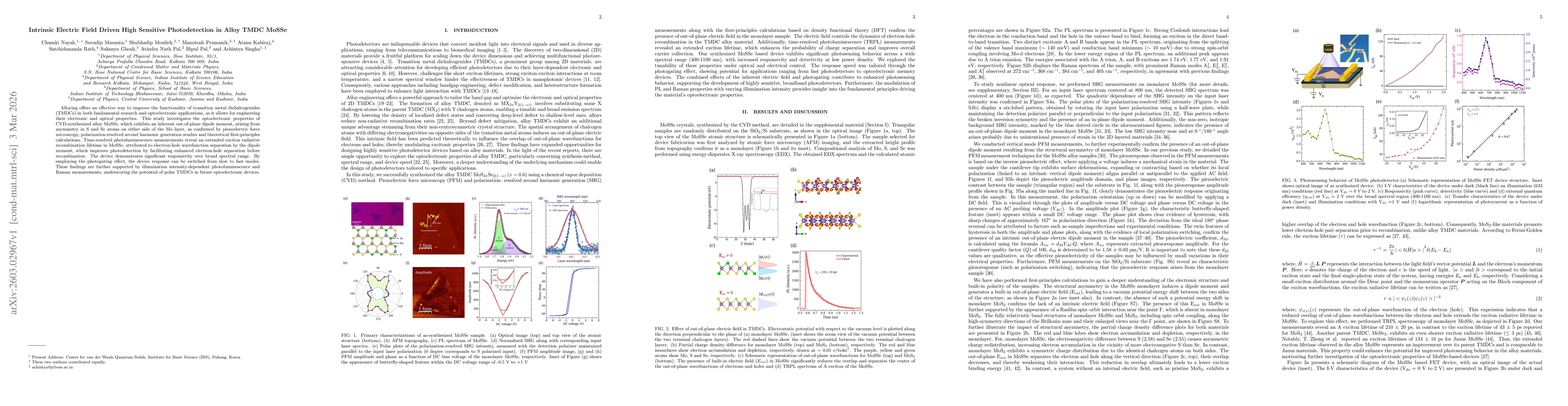
Alloying offers an effective way to improve the functionality of transition metal dichalcogenides (TMDCs) in both fundamental research and optoelectronic applications, as it allows for engineering their electronic and optical properties. This study investigates the optoelectronic properties of CVD-synthesized alloy MoSSe, which exhibits an inherent out-of-plane dipole moment, arising from asymmetry in S and Se atoms on either side of the Mo layer, as confirmed by piezoelectric force microscopy, polarization-resolved second harmonic generation studies and theoretical first-principles calculations. Time-resolved photoluminescence measurements reveal an extended exciton radiative recombination lifetime in MoSSe, attributed to electron-hole wavefunction separation by the dipole moment, which improves photodetection by facilitating enhanced electron-hole separation before recombination. The device demonstrates significant responsivity over broad spectral range. By employing the photogating effect, the device response can be switched from slow to fast modes. These findings are further supported by illumination intensity-dependent photoluminescence and Raman measurements, underscoring the potential of polar TMDCs in future optoelectronic devices.
Key Findings, in focus

Seven facets of this paper, analysed and brought into focus by AI.

AI-generated · verify against source Generated Mar 04, 2026
In focus · one-line synthesis

Demonstrates that alloying to create Janus MoSSe provides a tunable internal electric field that can be harnessed for ultra‑sensitive, broadband photodetectors with controllable temporal response, opening avenues for compact spectroscopy and threat‑detection devices.

01
MethodologyHow they did it

CVD growth of monolayer MoSSe alloy followed by AFM, EDX, SHG, PFM, PL, Raman, and TRPL characterization; device fabrication with Au contacts and electrical/optical testing; first‑principles DFT calculations to confirm dipole and Rashba splitting.

02
ResultsWhat they found
  • Intrinsic out‑of‑plane dipole in MoSSe enhances exciton lifetime and enables high responsivity (mA/W) across visible to IR at room temperature.
  • Photogating via hole trapping allows switching between slow (ms) and fast (µs) photodetection modes by varying illumination intensity.
  • Trion formation and defect passivation at higher light powers increase carrier density and further boost photocurrent, supported by PL and Raman studies.
03
SignificanceWhy it matters

Demonstrates that alloying to create Janus MoSSe provides a tunable internal electric field that can be harnessed for ultra‑sensitive, broadband photodetectors with controllable temporal response, opening avenues for compact spectroscopy and threat‑detection devices.

04
Technical ContributionsWhat's new technically

First experimental evidence that an intrinsic out‑of‑plane dipole in a Janus TMDC can be exploited to achieve long carrier lifetimes, Rashba splitting, and tunable photogating in a single photodetector platform.

05
NoveltyWhat sets it apart

Combines alloy engineering, intrinsic electric field, and defect‑mediated photogating to realize a high‑sensitivity, broadband photodetector with switchable response, a capability not demonstrated in previous TMDC studies.

06
LimitationsWhat to be cautious about
  • Device performance evaluated only at room temperature; temperature dependence remains unexplored.
  • Long‑term stability and scalability of the CVD‑grown alloy films were not assessed.
07
Future WorkWhere it goes next
  • Investigate other MoSSe‑based alloy compositions and heterostructures to optimize responsivity and speed.
  • Study temperature and environmental effects on dipole strength, carrier lifetime, and device noise to enable practical deployment.

Paper Details

Paper ID: 2603.02967
Categories:
cond-mat.mtrl-sci cond-mat.mes-hall

How to Cite This Paper

Reference manager: RIS EndNote


Discussion 0

This website uses cookies to ensure you get the best experience. Learn more