ArxivLens
ArXiv physics.optics cond-mat.mes-hall physics.app-ph

Inverse-Designed Grating Couplers with Tunable Wavelength via Scaling and Biasing

Fabian Becker, Kai Müller, Lorenz J. J. Sauerzopf

2510.27476 Published Oct 31, 2025
View PDF

Publication

Published: Oct 31, 2025
Categories: physics.optics, cond-mat.mes-hall, physics.app-ph

Metrics

Source: ArXiv

Quick Answers

What methodology did the authors use?

The research employed inverse design techniques using Lumerical FDTD and lumopt optimizer to create grating couplers. They fabricated and tested devices using a 4f-scanning setup, applying scaling and edge biasing to adjust for fabrication variations. More in Methodology →

What are the key results?

Inverse-designed grating couplers achieved up to 46% efficiency at shifted wavelengths. — Systematic scaling and edge biasing improved efficiency by up to eightfold compared to unadjusted designs. More in Key Results →

Why is this work significant?

This work enables reliable, wafer-scale photonic integration with tunable wavelength capabilities, crucial for telecommunication, biosensing, and quantum technologies. It addresses fabrication variability issues through post-design adjustments. More in Significance →

What are the main limitations?

The InGaAs detector imposed a spectral cutoff at 1620nm, limiting broadband efficiency measurement. — Manual z-alignment introduced measurement variations. More in Limitations →

Paper Preview

Abstract

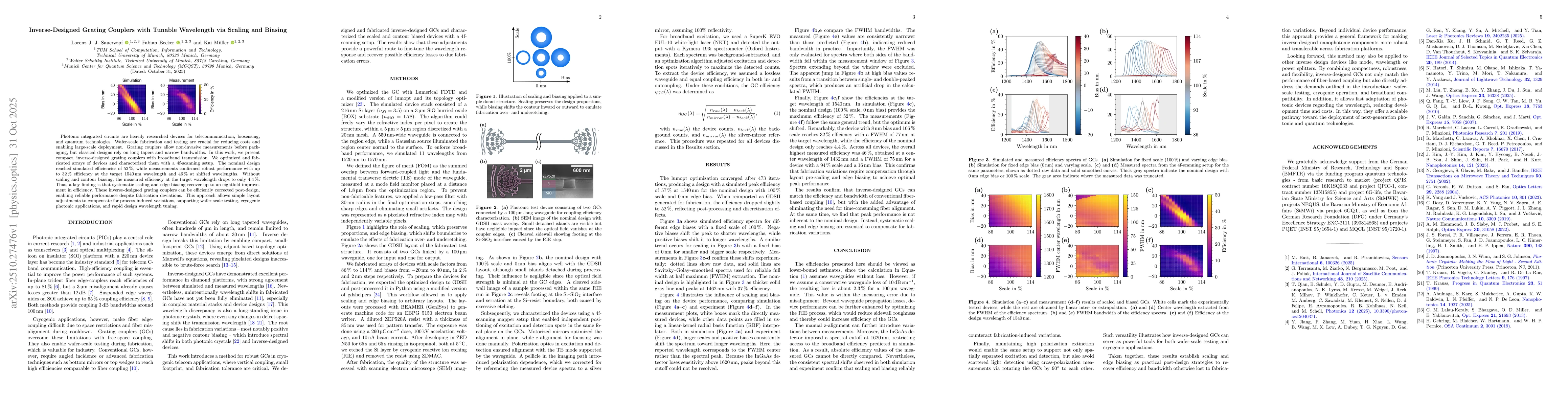
Photonic integrated circuits are heavily researched devices for telecommunication, biosensing, and quantum technologies. Wafer-scale fabrication and testing are crucial for reducing costs and enabling large-scale deployment. Grating couplers allow non-invasive measurements before packaging, but classical designs rely on long tapers and narrow bandwidths. In this work, we present compact, inverse-designed grating couplers with broadband transmission. We optimized and fabricated arrays of devices and characterized them with a 4f-scanning setup. The nominal design reached simulated efficiencies of 52 %, while measurements confirmed robust performance with up to 32 % efficiency at the target 1540 nm wavelength and 46 % at shifted wavelengths. Without scaling and contour biasing, the measured efficiency at the target wavelength drops to only 4.4 %. Thus, a key finding is that systematic scaling and edge biasing recover up to an eightfold improvement in efficiency. These inverse-designed grating couplers can be efficiently corrected post-design, enabling reliable performance despite fabrication deviations. This approach allows simple layout adjustments to compensate for process-induced variations, supporting wafer-scale testing, cryogenic photonic applications, and rapid design wavelength tuning.

Key Findings, in focus

Seven facets of this paper, analysed and brought into focus by AI.

AI-generated · verify against source Generated Nov 06, 2025
In focus · one-line synthesis

This work enables reliable, wafer-scale photonic integration with tunable wavelength capabilities, crucial for telecommunication, biosensing, and quantum technologies.

01
MethodologyHow they did it

The research employed inverse design techniques using Lumerical FDTD and lumopt optimizer to create grating couplers. They fabricated and tested devices using a 4f-scanning setup, applying scaling and edge biasing to adjust for fabrication variations.

02
ResultsWhat they found
  • Inverse-designed grating couplers achieved up to 46% efficiency at shifted wavelengths.
  • Systematic scaling and edge biasing improved efficiency by up to eightfold compared to unadjusted designs.
  • Efficiency at target wavelength (1540nm) reached 32% with scaling and biasing, versus 4.4% without.
03
SignificanceWhy it matters

This work enables reliable, wafer-scale photonic integration with tunable wavelength capabilities, crucial for telecommunication, biosensing, and quantum technologies. It addresses fabrication variability issues through post-design adjustments.

04
Technical ContributionsWhat's new technically

Development of inverse-designed grating couplers with post-design scaling and edge biasing to compensate for fabrication variations, achieving broadband and tunable wavelength performance.

05
NoveltyWhat sets it apart

The use of systematic scaling and edge biasing as post-design corrections for fabrication errors, combined with inverse design methods, provides a practical solution for wafer-scale photonic integration with tunable wavelength capabilities.

06
LimitationsWhat to be cautious about
  • The InGaAs detector imposed a spectral cutoff at 1620nm, limiting broadband efficiency measurement.
  • Manual z-alignment introduced measurement variations.
  • Absolute efficiency comparisons are challenging due to waveguide loss assumptions.
07
Future WorkWhere it goes next
  • Optimizing RIE processes to reduce sidewall roughness and improve efficiency.
  • Extending the approach to other inverse-designed photonic components like splitters.
  • Exploring cross-polarization measurements for scattered light detection.
  • Developing automated alignment techniques to reduce manual variations.

Paper Details

Paper ID: 2510.27476
Categories:
physics.optics cond-mat.mes-hall physics.app-ph

How to Cite This Paper

Reference manager: RIS EndNote


Discussion 0

This website uses cookies to ensure you get the best experience. Learn more