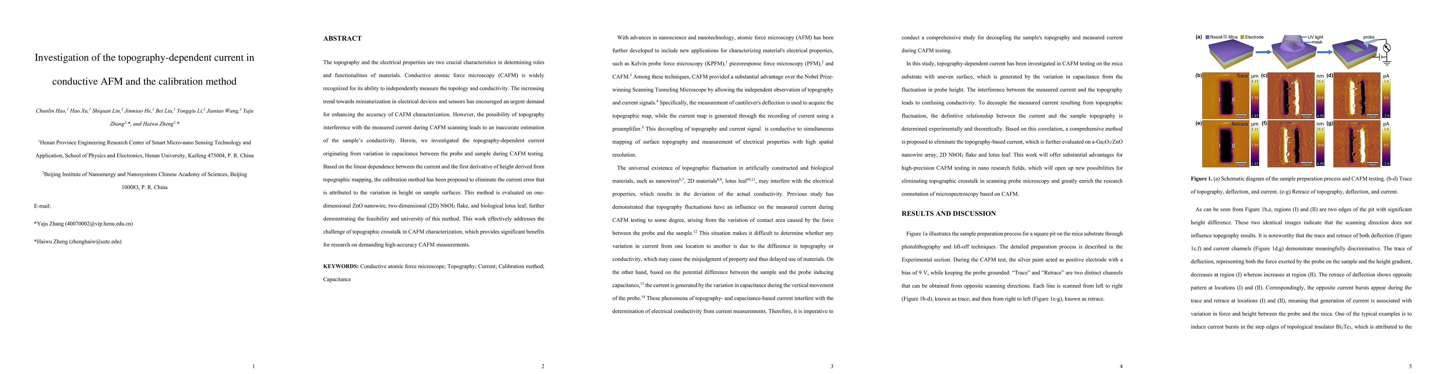
Ferroelectricity in Niobium Oxide Dihalides NbOX2 (X = Cl, I): A Macroscopic- to Microscopic-Scale Study.
|
Chaofei Liu, Xiuying Zhang, Xinyun Wang, Ziying Wang, Ibrahim Abdelwahab, I. Verzhbitskiy, Y. Shao, G. Eda, Wanxin Sun, L. Shen, K. Loh
|
2023
|
View Paper
|
Piezo-phototronic effect regulated broadband photoresponse of a-Ga2O3/ZnO heterojunction.
|
Jiantao Wang, Yan Zhou, Zihan Wang, Boying Wang, Yongqiu Li, Banghao Wu, Chunlin Hao, Yaju Zhang, Haiwu Zheng
|
2023
|
View Paper
|
An ultraweak mechanical stimuli actuated single electrode triboelectric nanogenerator with high energy conversion efficiency.
|
Yi Lv, Tianzhao Bu, Hang-yu Zhou, Guoxu Liu, Yunkang Chen, Zhaozheng Wang, Xianpeng Fu, Yuan Lin, Jie Cao, Chi Zhang
|
2022
|
View Paper
|
Bioinspired Hybrid Micro/Nanostructure Composited Membrane with Intensified Mass Transfer and Antifouling for High Saline Water Membrane Distillation.
|
Xiaobin Jiang, Yushan Shao, Jin Li, Mengyuan Wu, Y. Niu, X. Ruan, Xiaoming Yan, Xiangcun Li, G. He
|
2020
|
View Paper
|
Enhanced Photovoltaic Performances of La-Doped Bismuth Ferrite/Zinc Oxide Heterojunction by Coupling Piezo-Phototronic Effect and Ferroelectricity.
|
Yuanzheng Zhang, Liya Yang, Yaju Zhang, Zhenyu Ding, Mengjun Wu, Yan Zhou, C. Diao, Haiwu Zheng, Xingfu Wang, Zhong Lin Wang
|
2020
|
View Paper
|
Flexoelectronics of centrosymmetric semiconductors
|
Longfei Wang, Shuhai Liu, Xiaolong Feng, Chunli Zhang, Laipan Zhu, J. Zhai, Yong Qin, Zhong Lin Wang
|
2020
|
View Paper
|
Piezotronic Tunneling Junction Gated by Mechanical Stimuli
|
Shuhai Liu, Longfei Wang, Xiaolong Feng, Jinmei Liu, Yong Qin, Zhong Lin Wang
|
2019
|
View Paper
|
Conductive Atomic Force Microscopy
|
Wesley C. Sanders
|
2019
|
View Paper
|
Scanning probe microscopy for advanced nanoelectronics
|
F. Hui, M. Lanza
|
2019
|
View Paper
|
Excluding Contact Electrification in Surface Potential Measurement Using Kelvin Probe Force Microscopy.
|
Shengming Li, Yusheng Zhou, Yunlong Zi, Gong Zhang, Zhong Lin Wang
|
2016
|
View Paper
|
Nanoscale Probing of Local Electrical Characteristics on MBE-Grown Bi₂Te₃ Surfaces under Ambient Conditions.
|
R. Macedo, S. Harrison, T. Dorofeeva, J. Harris, R. Kiehl
|
2015
|
View Paper
|
Vapour-mediated sensing and motility in two-component droplets
|
Nate J. Cira, Adrien Benusiglio, Manu Prakash
|
2015
|
View Paper
|
In situ quantitative study of nanoscale triboelectrification and patterning.
|
Yu Sheng Zhou, Yuehan Liu, G. Zhu, Zong‐Hong Lin, Caofeng Pan, Qingshen Jing, Zhong Lin Wang
|
2013
|
View Paper
|
Correlation between the nanoscale electrical and morphological properties of crystallized hafnium oxide-based metal oxide semiconductor structures
|
V. Iglesias, M. Porti, M. Nafría, X. Aymerich, P. Dudek, T. Schroeder, G. Bersuker
|
2010
|
View Paper
|
Nanoscale electrical properties of cluster-assembled palladium oxide thin films
|
V. Cassina, L. Gerosa, A. Podestà, G. Ferrari, M. Sampietro, F. Fiorentini, T. Mazza, C. Lenardi, P. Milani
|
2009
|
View Paper
|
Nanoscale capacitance imaging with attofarad resolution using ac current sensing atomic force microscopy
|
L. Fumagalli, G. Ferrari, M. Sampietro, Ignacio Casuso, Elena Martínez, Josep Samitier, Gabriel Gomila
|
2006
|
View Paper
|
Piezoelectric Nanogenerators Based on Zinc Oxide Nanowire Arrays
|
Zhong Lin Wang, Jinhui Song
|
2006
|
View Paper
|
Spatially resolved electrical measurements of SiO2 gate oxides using atomic force microscopy
|
M. Murrell, M. Welland, S. O’Shea, T. Wong, J. Barnes, A. McKinnon, M. Heyns, S. Verhaverbeke
|
1993
|
View Paper
|
Local poling of ferroelectric polymers by scanning force microscopy
|
P. Guethner, K. Dransfeld
|
1992
|
View Paper
|
Influence of parasitic capacitances on conductive AFM I-V measurements and approaches for its reduction
|
M. Rommel, J. Jambreck, M. Lemberger, A. Bauer, L. Frey, K. Murakami, C. Richter, P. Weinzierl
|
2013
|
View Paper
|
Kelvin Probe Force Microscopy
|
|
|
View Paper
|
2D NbOI 2 : A Chiral Semiconductor with Highly In-Plane Anisotropic Electrical and Optical Properties
|
|
|
|
1. (a) schematic diagram of the sample preparation process and CAFM testing
|
|
|
|
Comments (0)