Ion-Beam-Induced Defects in CMOS Technology: Methods of Study
Publication
Metrics
Paper Preview
Abstract
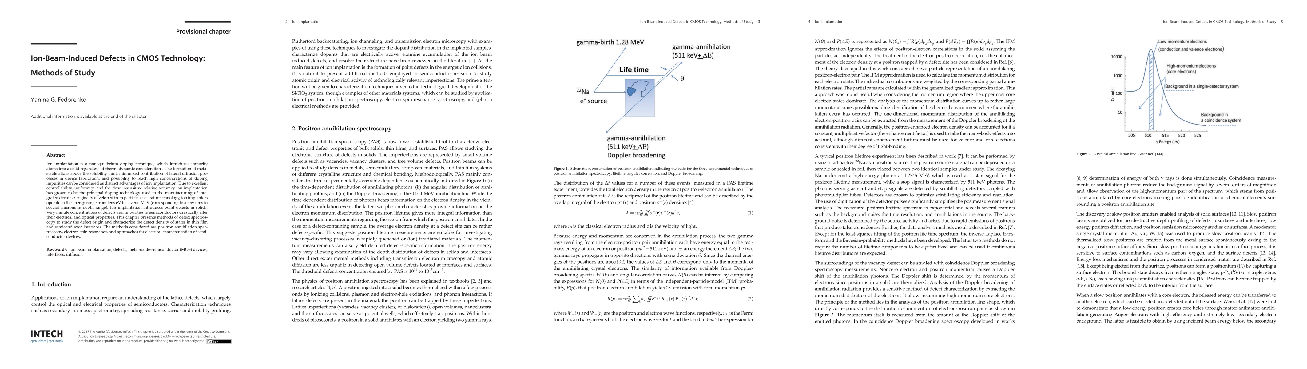
Ion implantation is a non-equilibrium doping technique which introduces impurity atoms into a solid regardless of thermodynamic considerations. The formation of metastable alloys above the solubility limit, minimized contribution of lateral diffusion processes in device fabrication, and possibility to reach high concentrations of doping impurities can be considered as distinct advantages of ion implantation. Owing to excellent controllability, uniformity, and the dose insensitive relative accuracy ion implantation has grown to be the principal doping technology used in the manufacturing of integrated circuits. Originally developed from particle accelerator technology ion implanters operate in the energy range from tens eV to several MeV (corresponding to a few nm to several microns in depth). The main feature of ion implantation is the formation of point defects in the energetic ion collisions. Very minute concentrations of defects and impurities in semiconductors drastically alter their electrical and optical properties. This chapter presents methods of defect spectroscopy to study the defect origin and characterize the defect density of states in thin film and semiconductor interfaces. The methods considered are positron annihilation spectroscopy, electron spin resonance, and approaches for electrical characterization of semiconductor devices.
AI Key Findings
Get AI-generated insights about this paper's methodology, results, significance, and more — seven facets brought into focus.
Impact
Paper Details
PDF Preview
Key Terms
Citation Network
Current paper (gray), citations (green), references (blue)
Display is limited for performance on very large graphs.
Discussion 0