01
MethodologyHow they did it
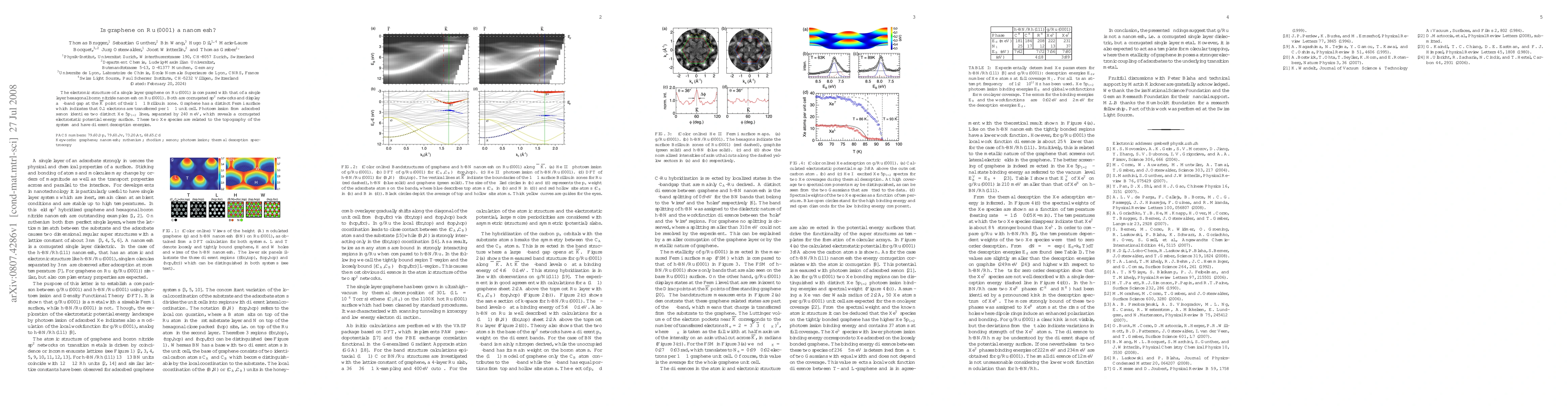
The research methodology involved ab initio calculations with the VASP package based on DFT, PAW pseudo-potentials, and the PBE exchange-correlation functional in the GGA. Bandstructure calculations were performed for epitaxial (1×1) CorB/Ru structures with a lattice constant of graphene, a 4-layer Ru slab, a 36×36×1 k-sampling, and a 400 eV cutoff. Large moiré periodicities were considered for atomic structure and electrostatic potential calculations.
Discussion 0