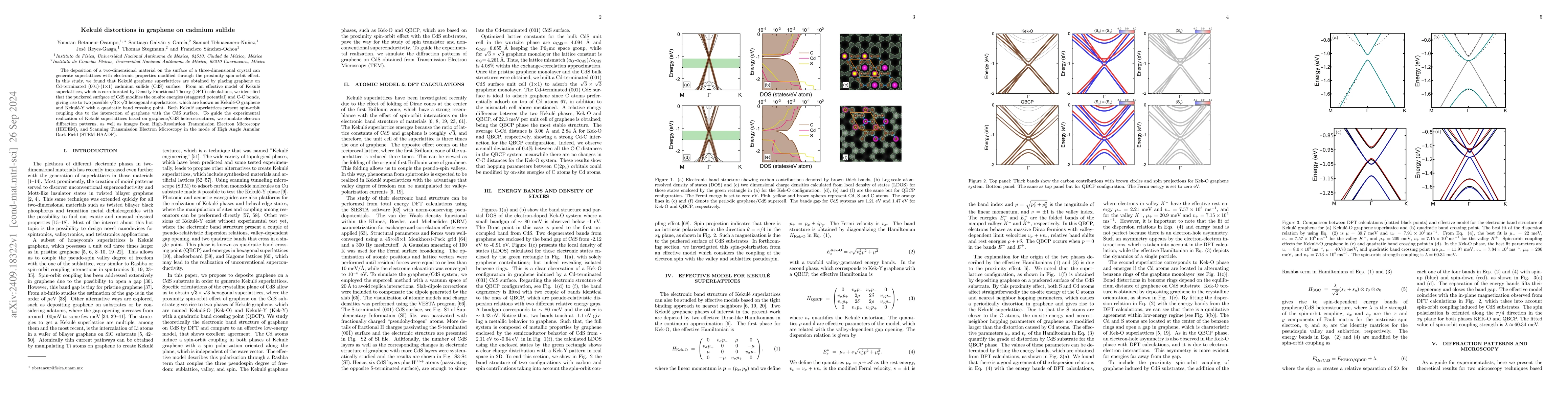
The deposition of a two-dimensional material on the surface of a
three-dimensional crystal can generate superlattices with electronic properties
modified through the proximity spin-orbit effect. In this study, we found that
Kekul\'e graphene superlattices are obtained by placing graphene on
Cd-terminated (001)-(1$\times$1) cadmium sulfide (CdS) surface. From an
effective model of Kekul\'e superlattices, which is corroborated by Density
Functional Theory (DFT) calculations, we identified that the puckered surfqace
of CdS modifies the on-site energies (staggered potential) and C-C bonds,
giving rise to two possible $\sqrt{3} \times \sqrt{3}$ hexagonal superlattices,
which are known as Kekul\'e-O graphene and Kekul\'e-Y with a quadratic band
crossing point. Both Kekul\'e superlattices present spin-orbit coupling due to
the interaction of graphene with the CdS surface. To guide the experimental
realization of Kekul\'e superlattices based on graphene/CdS heterostructures,
we simulate electron diffraction patterns, as well as images from
High-Resolution Transmission Electron Microscopy (HRTEM), and Scanning
Transmission Electron Microscopy in the mode of High Angle Annular Dark Field
(STEM-HAADF).
Discussion 0