Publication
Metrics
AI Quick Summary
Researchers have developed a 0.2 um fully-depleted SOI technology for X-ray pixel detectors, improving performance with advanced process techniques and novel structure designs.
Paper Preview
Abstract
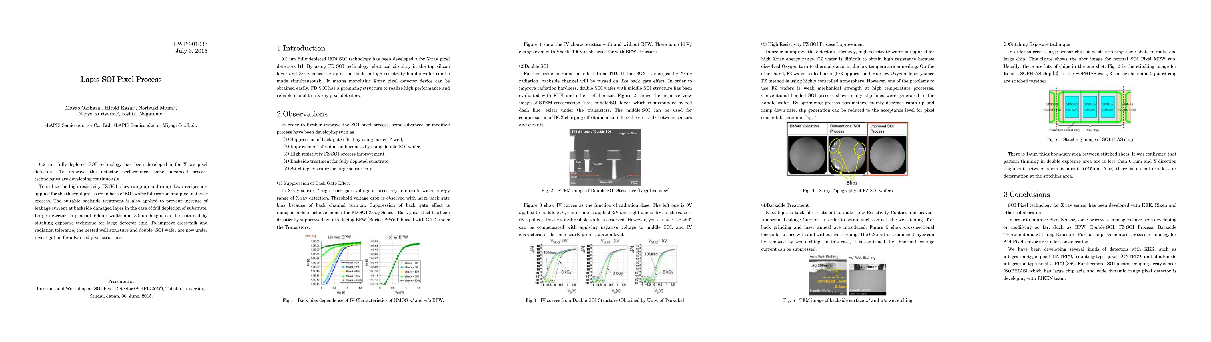
0.2 um fully-depleted SOI technology has been developed a for X-ray pixel detectors. To improve the detector performance, some advanced process technologies are developing continuously. To utilize the high resistivity FZ-SOI, slow ramp up and ramp down recipes are applied for the thermal processes in both of SOI wafer fabrication and pixel detector process. The suitable backside treatment is also applied to prevent increase of leakage current at backside damaged layer in the case of full depletion of substrate. Large detector chip about 66mm width and 30mm height can be obtained by stitching exposure technique for large detector chip. To improve cross-talk and radiation tolerance, the nested well structure and double- SOI wafer are now under investigation for advanced pixel structure.
AI Key Findings
Get AI-generated insights about this paper's methodology, results, significance, and more — seven facets brought into focus.
Paper Details
PDF Preview
Key Terms
Related Papers
No references found for this paper.
Discussion 0