01
MethodologyHow they did it
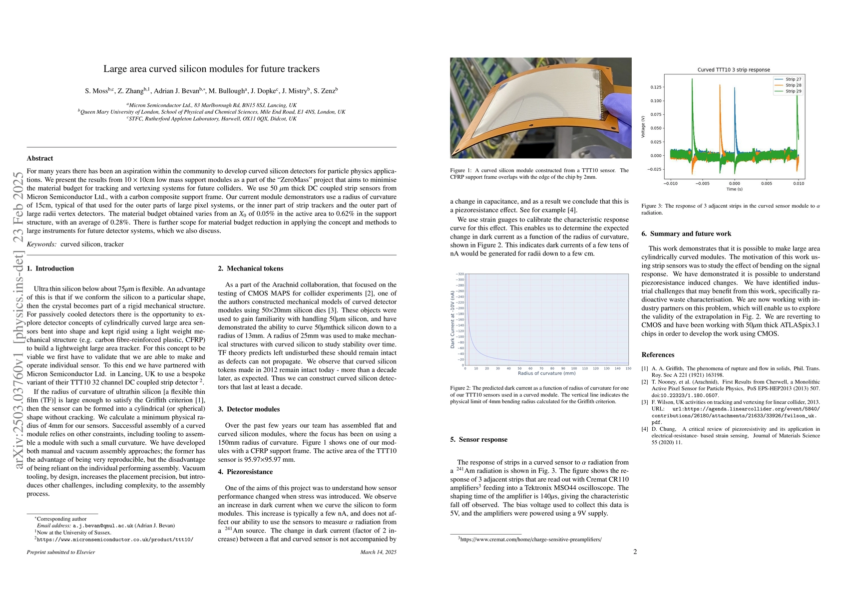
The research utilized 50 µm thick DC coupled strip sensors from Micron Semiconductor Ltd., with a carbon composite support frame, to create 10 x 10 cm low mass support modules. The modules were designed with a radius of curvature of 15 cm, typical for outer parts of large pixel systems or inner parts of strip trackers and outer parts of large radius vertex detectors.
Discussion 0