Summary
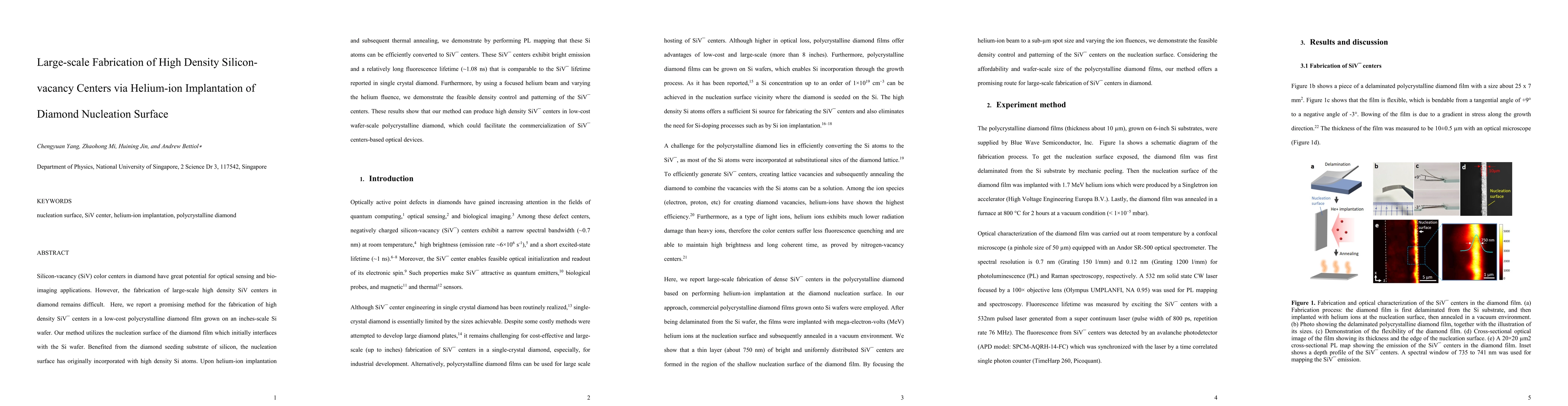
Silicon-vacancy (SiV) color centers in diamond have great potential for optical sensing and bio-imaging applications. However, the fabrication of large-scale high-density SiV centers in diamond remains difficult. Here, we report a promising method for the fabrication of high-density SiV- centers in a low-cost polycrystalline diamond film grown on an inches-scale Si wafer. Our method utilizes the nucleation surface of the diamond film which initially interfaces with the Si wafer. Benefited from the diamond seeding substrate of silicon, the nucleation surface has originally been incorporated with high-density Si atoms. Upon helium-ion implantation and subsequent thermal annealing, we demonstrate by performing PL mapping that these Si atoms can be efficiently converted to SiV- centers. The SiV- centers exhibit bright emission and a relatively long fluorescence lifetime (~1.08 ns) that is comparable to the SiV- lifetime reported in single-crystal diamonds. Furthermore, by using a focused helium beam and varying the helium fluence, we demonstrate the feasible density control and patterning of the SiV- centers. These results show that our method can produce high-density SiV- centers in low-cost wafer-scale polycrystalline diamonds, which could facilitate the commercialization of SiV- centers-based optical devices.
AI Key Findings
Generated Sep 02, 2025
Methodology
The research utilized helium-ion implantation on a silicon-seeded polycrystalline diamond film grown on a Si wafer, followed by thermal annealing to convert Si atoms to SiV- centers.
Key Results
- High-density SiV- centers (up to 10^18 cm^-3) were fabricated in a low-cost polycrystalline diamond film.
- Efficient conversion of Si to SiV- centers was demonstrated by photoluminescence (PL) mapping and spectroscopy.
- Bright emission and a long fluorescence lifetime (~1.08 ns) comparable to single-crystal diamonds were observed for SiV- centers.
- Density control and patterning of SiV- centers were achieved using a focused helium beam.
- The method enables the production of high-density SiV- centers in wafer-scale polycrystalline diamonds, facilitating commercialization of SiV- centers-based optical devices.
Significance
This research presents a promising method for large-scale fabrication of high-density SiV- centers in low-cost polycrystalline diamonds, which is crucial for the development of commercial optical devices for sensing and bio-imaging applications.
Technical Contribution
The paper introduces a novel method for large-scale fabrication of high-density SiV- centers in polycrystalline diamond films via helium-ion implantation and thermal annealing, demonstrating efficient conversion of Si atoms to SiV- centers with controlled density and patterning.
Novelty
This work stands out by presenting a low-cost method for producing high-density SiV- centers in polycrystalline diamond films, which is a significant advancement over existing techniques limited to single-crystal diamonds, paving the way for commercial applications in optical sensing and bio-imaging.
Limitations
- The study was conducted on polycrystalline diamond films, which may have inherent mechanical and optical properties differences compared to single-crystal diamonds.
- The long-term stability and reliability of SiV- centers in these polycrystalline films under various environmental conditions were not explored.
Future Work
- Investigate the long-term stability and reliability of SiV- centers in polycrystalline diamond films.
- Explore the scalability of this method for even larger diamond substrates and its applicability to other color centers in diamond.
Paper Details
PDF Preview
Key Terms
Citation Network
Current paper (gray), citations (green), references (blue)
Display is limited for performance on very large graphs.
Similar Papers
Found 4 papersEfficient fabrication of high-density ensembles of color centers via ion implantation on a hot diamond substrate
G. Andrini, S. Ditalia Tchernij, E. Corte et al.
No citations found for this paper.
Comments (0)