Publication
Metrics
AI Quick Summary
This paper investigates laser doping of crystalline Si substrates using B-doped Si nanoparticles, achieving uniform doping profiles and significant conductivity increases via laser annealing. The method also successfully creates pn-diodes by doping n-type Si substrates.
Paper Preview
Abstract
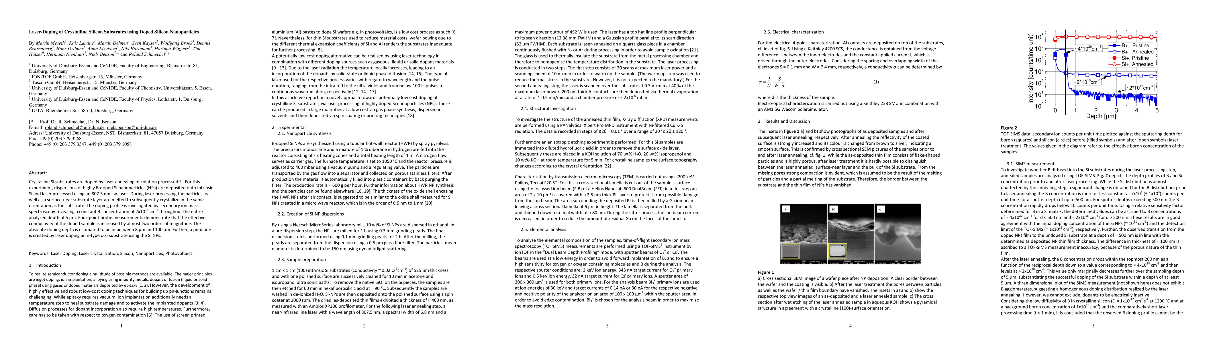
Crystalline Si substrates are doped by laser annealing of solution processed Si. For this experiment, dispersions of highly B-doped Si nanoparticles (NPs) are deposited onto intrinsic Si and laser processed using an 807.5nm cw-laser. During laser processing the particles as well as a surface-near substrate layer are melted to subsequently crystallize in the same orientation as the substrate. The doping profile is investigated by secondary ion mass spectroscopy revealing a constant B concentration of 2x10^18 cm^-3 throughout the entire analyzed depth of 5\mu m. Four-point probe measurements demonstrate that the effective conductivity of the doped sample is increased by almost two orders of magnitude. The absolute doping depth is estimated to be in between 8\mu m and 100\mu m. Further, a pn-diode is created by laser doping an n-type c-Si substrate using the Si NPs.
AI Key Findings
Get AI-generated insights about this paper's methodology, results, significance, and more — seven facets brought into focus.
Impact
Paper Details
PDF Preview
Key Terms
Citation Network
Current paper (gray), citations (green), references (blue)
Display is limited for performance on very large graphs.
Discussion 0