Summary
In recent years, two-dimensional (2D) layered semiconductors have received much attention for their potential in next-generation electronics and optoelectronics. Wide-bandgap 2D semiconductors are especially important in blue and ultraviolet wavelength region, while there are very few 2D materials in this region. Here, monolayer \b{eta}-type zirconium nitride chloride (\b{eta}-ZrNCl) is isolated for the first time, which is an air-stable layered material with a bandgap of ~3.0 eV in bulk. Systematical investigation of layer-dependent Raman scattering of ZrNCl from monolayer, bilayer, to bulk reveals a blue shift of its out-of-plane A1g peak at ~189 cm-1. Importantly, this A1g peak is absent in monolayer, suggesting that it is a fingerprint to quickly identify monolayer and for the thickness determination of 2D ZrNCl. The back-gate field-effect transistor based on few-layer ZrNCl shows a high on/off ratio of 108. These results suggest the potential of 2D \b{eta}-ZrNCl for electronic applications.
AI Key Findings
Get AI-generated insights about this paper's methodology, results, and significance.
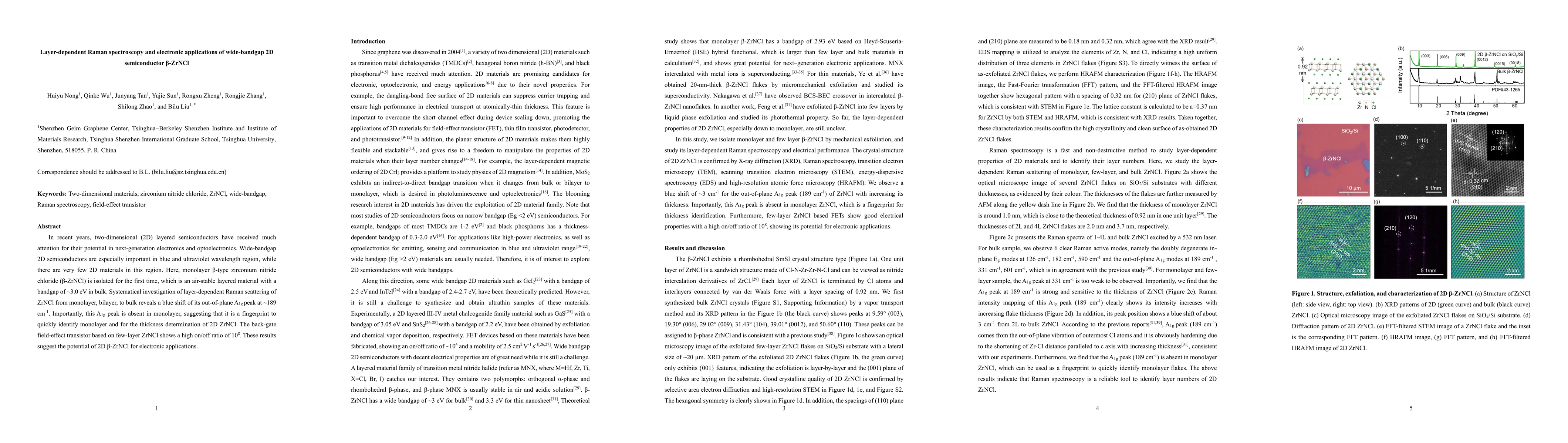
Paper Details
PDF Preview
Key Terms
Citation Network
Current paper (gray), citations (green), references (blue)
Display is limited for performance on very large graphs.
Similar Papers
Found 4 papersExploring Layer Thinning of Exfoliated \b{eta}-Tellurene and Room Temperature Photoluminescence with Large Exciton Binding Energy Revealed in TeO2
Frank W. DelRio, Sarah Alsaggaf, Thamer Tabbakh et al.
Thermal conversion of ultrathin nickel hydroxide for wide bandgap 2D nickel oxides
Zifan Wang, Nicholas Russo, Xi Ling et al.
| Title | Authors | Year | Actions |
|---|
Comments (0)