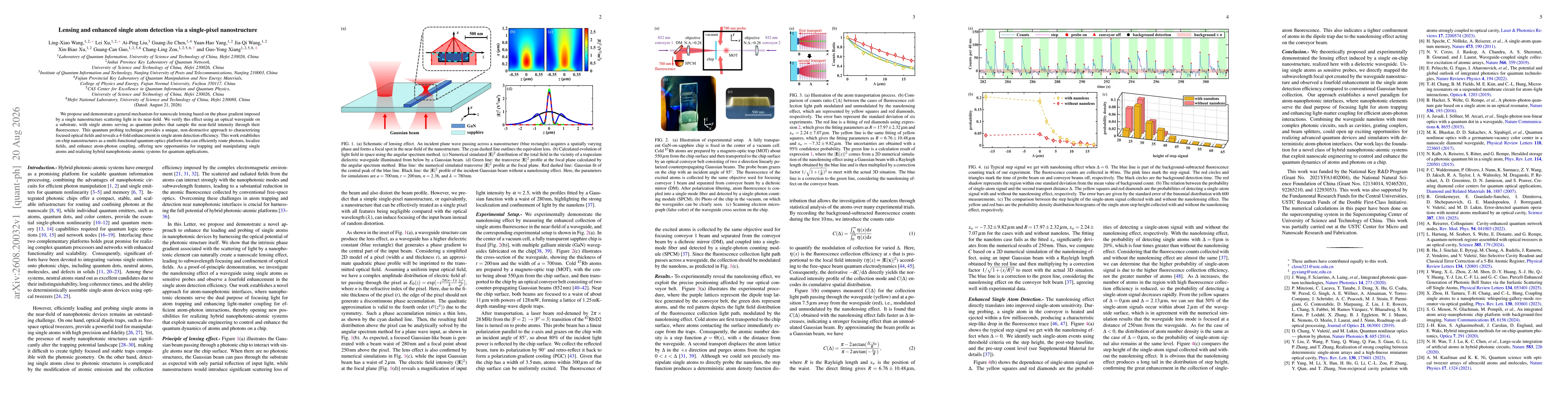
The study demonstrates nanoscale lensing via a single nanostructure by leveraging the phase gradient it imposes on incident light. A simplified 2D model treats the nanostructure as a single-pixel element imprinting a quadratic phase to the transmitted field, producing a focal spot above the structure. Numerical angular spectrum methods and simulations validate a focal localization (~280 nm waist) and a 4-fold enhancement in single-atom fluorescence collection, using a GaN waveguide on sapphire and a cold 87Rb atom ensemble in a MOT for probing near-field intensity.
Lensing and enhanced single atom detection via a single-pixel nanostructure
Publication
Metrics
Quick Answers
What methodology did the authors use?
The study demonstrates nanoscale lensing via a single nanostructure by leveraging the phase gradient it imposes on incident light. A simplified 2D model treats the nanostructure as a single-pixel element imprinting a quadratic phase to the transmitted field, producing a focal spot above the structure. Numerical angular spectrum methods and simulations validate a focal localization (~280 nm waist) and a... More in Methodology →
What are the key results?
A single-pixel nanostructure (nanolens) can focus an incident beam into a near-field focal region with a waist ~280 nm located ~250 nm above the nanostructure, indicating nanoscale light confinement. — Numerical simulations show a transverse intensity profile at the focal plane with a strong localization (approximate magnification of input light by α ≈ 2.5). More in Key Results →
Why is this work significant?
This work provides a general, non-destructive method to characterize focused optical fields at the nanoscale by using single atoms as probes, and demonstrates a practical, on-chip platform where a simple nanostructure can simultaneously focus light and enhance light-matter interactions for quantum applications. More in Significance →
What are the main limitations?
The analysis relies on a simplified 2D quadratic phase approximation which may not capture all 3D aberrations of realistic nanostructures. — Experimental proof is demonstrated for a specific waveguide geometry and atomic species; generalization to other platforms requires further validation. More in Limitations →
Abstract
We propose and demonstrate a general mechanism for nanoscale lensing based on the phase gradient imposed by a single nanostructure scattering light in its near-field. We verify this effect using an optical waveguide on a substrate, with single atoms serving as quantum probes that sample the near-field intensity through their fluorescence. This quantum probing technique provides a unique, non-destructive approach to characterizing focused optical fields and reveals a 4-fold enhancement in single atom detection efficiency. This work establishes on-chip nanostructures as a multi-functional quantum optics platform that can efficiently route photons, localize fields, and enhance atom-photon coupling, offering new opportunities for trapping and manipulating single atoms and realizing hybrid nanophotonic-atomic systems for quantum applications.
Key Findings, in focus
Seven facets of this paper, analysed and brought into focus by AI.
This work provides a general, non-destructive method to characterize focused optical fields at the nanoscale by using single atoms as probes, and demonstrates a practical, on-chip platform where a simple nanostructure can simultaneously focus light and enhance light-matter interactions for quantum applications.
- A single-pixel nanostructure (nanolens) can focus an incident beam into a near-field focal region with a waist ~280 nm located ~250 nm above the nanostructure, indicating nanoscale light confinement.
- Numerical simulations show a transverse intensity profile at the focal plane with a strong localization (approximate magnification of input light by α ≈ 2.5).
- Experimentally, a 4-fold enhancement in single-atom fluorescence collection is observed when atoms sample the near-field of the on-chip nanostructure compared to without the nanolens.
- The nanolens enables on-chip nanophotonic control to route photons and enhance atom-photon coupling, suggesting potential for integrated hybrid quantum systems.
This work provides a general, non-destructive method to characterize focused optical fields at the nanoscale by using single atoms as probes, and demonstrates a practical, on-chip platform where a simple nanostructure can simultaneously focus light and enhance light-matter interactions for quantum applications.
Introduction and experimental validation of a nanoscale lensing mechanism produced by a single nanostructure, enabling subwavelength focusing in the near-field and enhanced atom detection on a photonic chip, coupled with a quantitative model using angular spectrum methods.
First demonstration of a nanoscale lensing effect created by a single-pixel nanostructure on a chip that both localizes light at subwavelength scales and boosts single-atom detection efficiency through enhanced near-field interactions.
- The analysis relies on a simplified 2D quadratic phase approximation which may not capture all 3D aberrations of realistic nanostructures.
- Experimental proof is demonstrated for a specific waveguide geometry and atomic species; generalization to other platforms requires further validation.
- Quantitative disentanglement of collection efficiency improvements from other noise sources in the near-field environment may be challenging.
- Extend the nanolens concept to different nanostructure geometries and materials to optimize focusing efficiency and bandwidth.
- Explore integration with diverse atomic species and trap configurations to generalize the enhancement of atom-photon coupling on chip.
- Investigate dynamic tunability of the focal properties via active control of the nanostructure or surrounding photonic environment.
Discussion 0