Publication
Metrics
AI Quick Summary
Researchers introduce a new strategy for optimizing electromagnetic devices using continuous material averaging, achieving high accuracy and low insertion loss in device design.
Paper Preview
Abstract
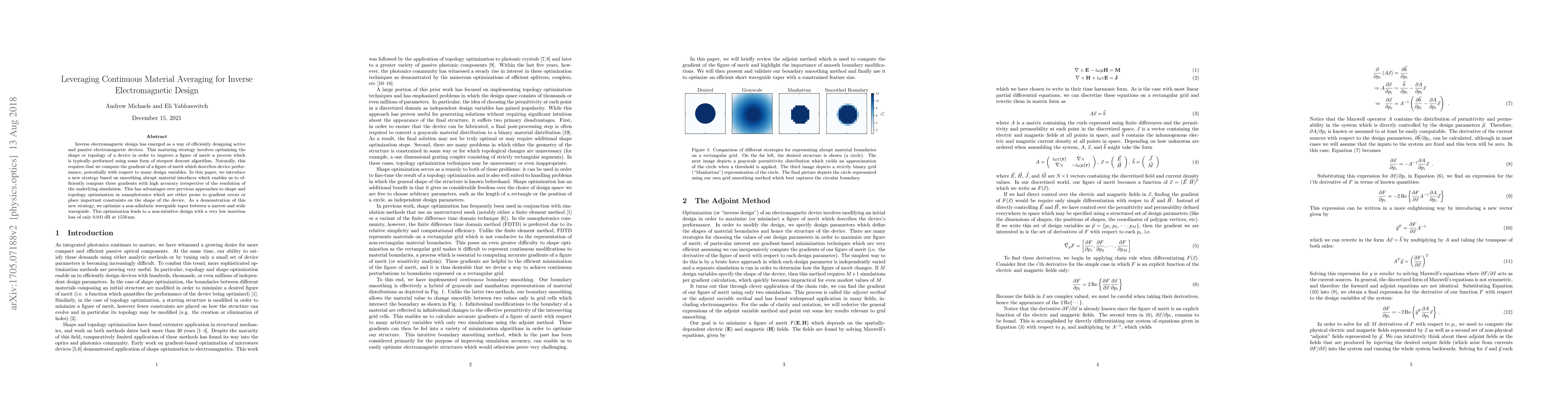
Inverse electromagnetic design has emerged as a way of efficiently designing active and passive electromagnetic devices. This maturing strategy involves optimizing the shape or topology of a device in order to improve a figure of merit--a process which is typically performed using some form of steepest descent algorithm. Naturally, this requires that we compute the gradient of a figure of merit which describes device performance, potentially with respect to many design variables. In this paper, we introduce a new strategy based on smoothing abrupt material interfaces which enables us to efficiently compute these gradients with high accuracy irrespective of the resolution of the underlying simulation. This has advantages over previous approaches to shape and topology optimization in nanophotonics which are either prone to gradient errors or place important constraints on the shape of the device. As a demonstration of this new strategy, we optimize a non-adiabatic waveguide taper between a narrow and wide waveguide. This optimization leads to a non-intuitive design with a very low insertion loss of only 0.041 dB at 1550 nm.
AI Key Findings
Get AI-generated insights about this paper's methodology, results, significance, and more — seven facets brought into focus.
Impact
Paper Details
PDF Preview
Key Terms
Citation Network
Current paper (gray), citations (green), references (blue)
Display is limited for performance on very large graphs.
Discussion 0