01
MethodologyHow they did it
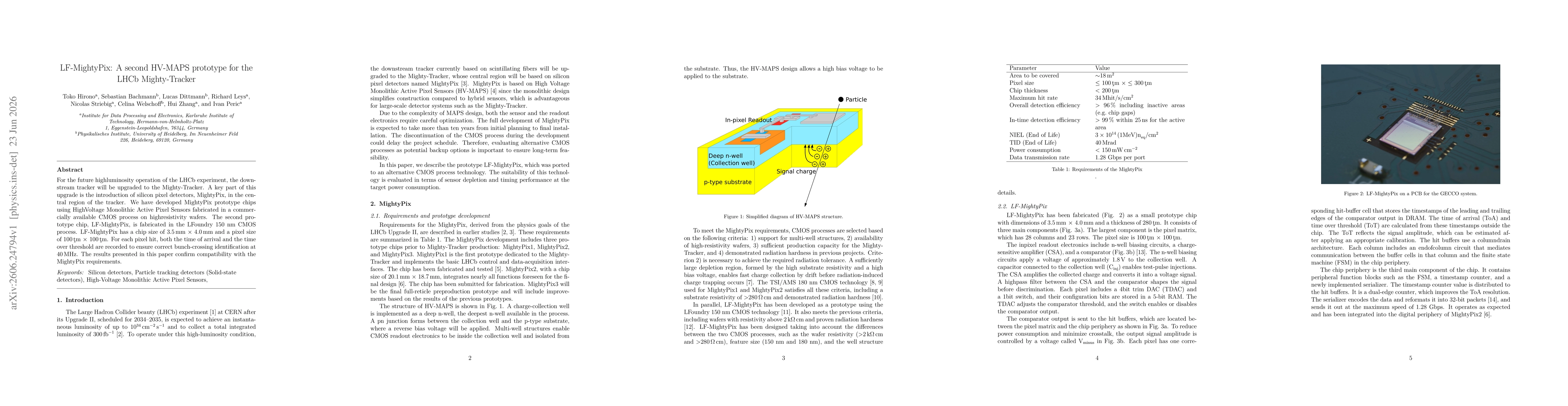
Prototype LF-MightyPix was ported to the LFoundry 150 nm CMOS process on high-resistivity wafers. The chip measures 3.5 mm x 4.0 mm with 0.1 mm x 0.1 mm pixels. For each pixel hit, both time of arrival and time over threshold were recorded to enable correct bunch-crossing identification at 40 MHz. Compatibility with MightyPix requirements was evaluated in terms of sensor depletion and timing performance at target power consumption.
Discussion 0