Light-Emitting Diodes with Micrometer-Thick Perovskite Charge Transport Layers
Publication
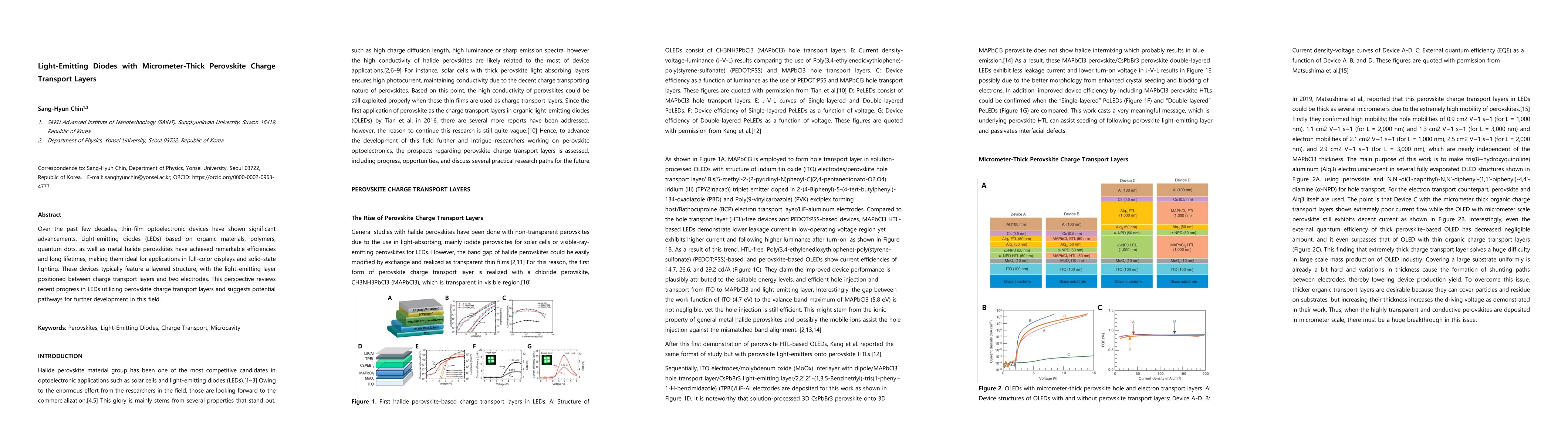
Metrics
Paper Preview
Abstract
Over the past few decades, thin-film optoelectronic devices have shown significant advancements. Light-emitting diodes (LEDs) based on organic materials, polymers, quantum dots, as well as metal halide perovskites have achieved remarkable efficiencies and long lifetimes, making them ideal for applications in full-color displays and solid-state lighting. These devices typically feature a layered structure, with the light-emitting layer positioned between charge transport layers and two electrodes. This perspective reviews recent progress in LEDs utilizing perovskite charge transport layers and suggests potential pathways for further development in this field.
AI Key Findings
Get AI-generated insights about this paper's methodology, results, significance, and more — seven facets brought into focus.
Discussion 0