Lithography-free patterning of chalcogenide materials for integrated photonic devices
Publication
Metrics
AI Quick Summary
This paper introduces a novel laser-induced localized oxidation technique for lithography-free patterning of chalcogenide materials, demonstrating its application in fabricating integrated photonic devices with high spatial resolution and refractive index contrast. This method simplifies the fabrication process and expands the practical applications of chalcogenide photonic devices.
Paper Preview
Abstract
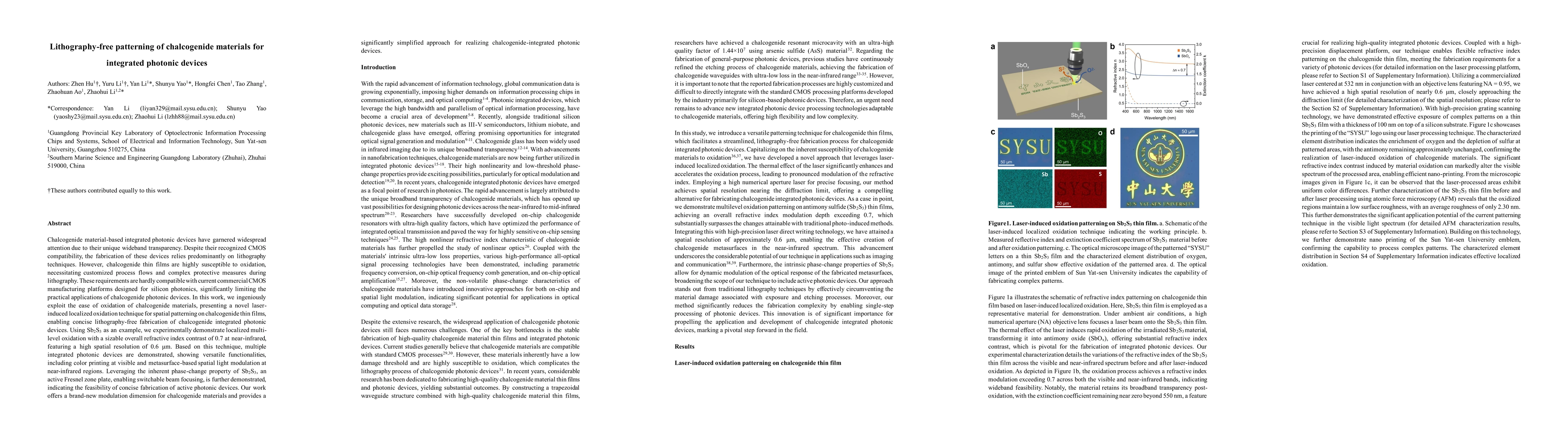
Chalcogenide material-based integrated photonic devices have garnered widespread attention due to their unique wideband transparency. Despite their recognized CMOS compatibility, the fabrication of these devices relies predominantly on lithography techniques. However, chalcogenide thin films are highly susceptible to oxidation, necessitating customized process flows and complex protective measures during lithography. These requirements are hardly compatible with current commercial CMOS manufacturing platforms designed for silicon photonics, significantly limiting the practical applications of chalcogenide photonic devices. In this work, we ingeniously exploit the ease of oxidation of chalcogenide materials, presenting a novel laser-induced localized oxidation technique for spatial patterning on chalcogenide thin films, enabling concise lithography-free fabrication of chalcogenide integrated photonic devices. Using Sb2S3 as an example, we experimentally demonstrate localized multi-level oxidation with a sizable overall refractive index contrast of 0.7 at near-infrared, featuring a high spatial resolution of 0.6 um. Based on this technique, multiple integrated photonic devices are demonstrated, showing versatile functionalities, including color printing at visible and metasurface-based spatial light modulation at near-infrared regions. Leveraging the inherent phase-change property of Sb2S3, an active Fresnel zone plate, enabling switchable beam focusing, is further demonstrated, indicating the feasibility of concise fabrication of active photonic devices. Our work offers a brand-new modulation dimension for chalcogenide materials and provides a significantly simplified approach for realizing chalcogenide-integrated photonic devices.
AI Key Findings
Get AI-generated insights about this paper's methodology, results, significance, and more — seven facets brought into focus.
Impact
Paper Details
Authors
PDF Preview
Citation Network
Current paper (gray), citations (green), references (blue)
Display is limited for performance on very large graphs.
Discussion 0