LNoS: Lithium Niobate on Silicon Spatial Light Modulator

PDF

Publication

Published: Feb 23, 2024
Categories: physics.optics, physics.app-ph, physics.ins-det

Metrics

Source: ArXiv

Quick Actions

View PDF

AI Quick Summary

This paper introduces a novel "Lithium Niobate on Silicon" (LNoS) spatial light modulator that integrates a megapixel-scale aperture with GHz-rate modulation speeds, leveraging a photonic crystal and guided mode resonance to achieve high-speed, programmable spatiotemporal light control. The proposed architecture aims to address current limitations in commercial SLMs and holds promise for advancements in optical communications, imaging, and quantum technologies.

Quick Answers

What is "LNoS: Lithium Niobate on Silicon Spatial Light Modulator" about?

This paper introduces a novel "Lithium Niobate on Silicon" (LNoS) spatial light modulator that integrates a megapixel-scale aperture with GHz-rate modulation speeds, leveraging a photonic crystal and guided mode resonance to achieve high-speed, programmable spatiotemporal light control. The proposed architecture aims to address current limitations in commercial SLMs and holds promise for advancements in optical communications, imaging, and quantum technologies.

What methodology did the authors use?

Fabricated a lithium niobate thin‑film photonic crystal resonator via electron‑beam and interference lithography, patterned gold electrodes, bonded the device to a commercial CMOS backplane using epoxy, and performed numerical simulations (FDTD, COMSOL, GME) and experimental optical measurements (cross‑polarized reflection, DC tuning, RF bandwidth with APD and lock‑in) to evaluate performance. More in Methodology →

What are the key results?

Achieved a 1.6‑GHz 3‑dB modulation bandwidth with a Q‑factor >1000 and 90% field overlap in a LN‑based guided‑mode resonance. — Demonstrated successful bonding of the LN photonic crystal to a megapixel CMOS backplane, enabling scalable spatial light modulation. More in Key Results →

Why is this work significant?

The work provides a scalable, GHz‑rate spatial light modulator that bridges the speed gap between conventional kHz SLMs and high‑speed modulators, opening possibilities for high‑speed imaging, quantum photonics, LiDAR, and AR/VR applications. More in Significance →

What are the main limitations?

Modulation depth is limited (~0.7%) by the small refractive‑index change and the epoxy bonding layer. — Performance is currently constrained by detector bandwidth and the thickness of the epoxy layer, which reduces field overlap. More in Limitations →

Paper Preview

Abstract

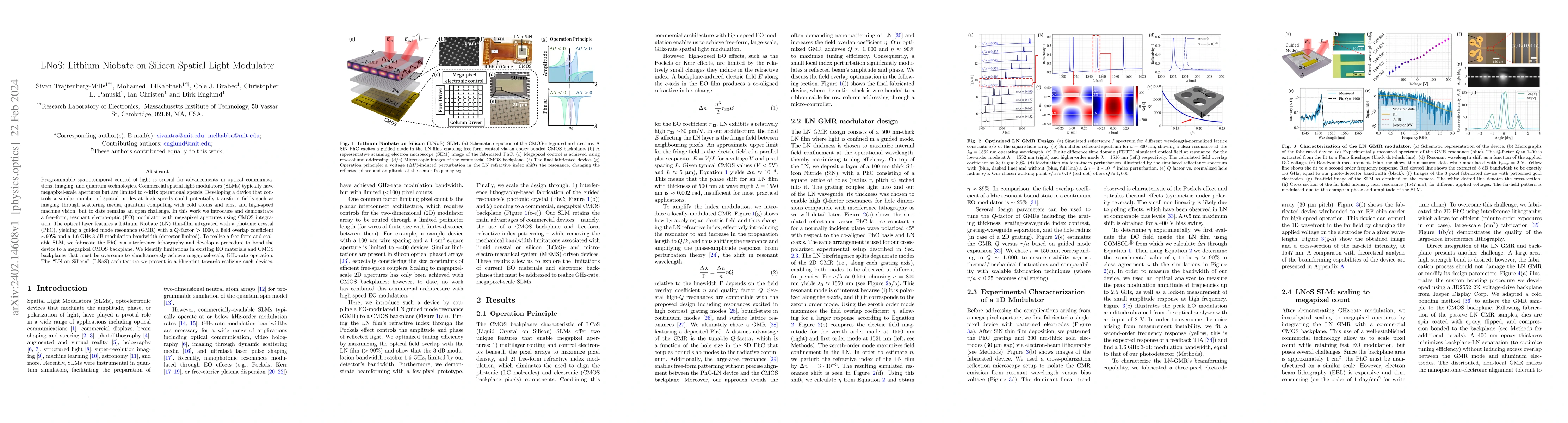
Programmable spatiotemporal control of light is crucial for advancements in optical communications, imaging, and quantum technologies. Commercial spatial light modulators (SLMs) typically have megapixel-scale apertures but are limited to ~kHz operational speeds. Developing a device that controls a similar number of spatial modes at high speeds could potentially transform fields such as imaging through scattering media, quantum computing with cold atoms and ions, and high-speed machine vision, but to date remains an open challenge. In this work we introduce and demonstrate a free-form, resonant electro-optic (EO) modulator with megapixel apertures using CMOS integration. The optical layer features a Lithium Niobate (LN) thin-film integrated with a photonic crystal (PhC), yielding a guided mode resonance (GMR) with a Q-factor>1000, a field overlap coefficient ~90% and a 1.6 GHz 3-dB modulation bandwidth (detector limited). To realize a free-form and scalable SLM, we fabricate the PhC via interference lithography and develop a procedure to bond the device to a megapixel CMOS backplane. We identify limitations in existing EO materials and CMOS backplanes that must be overcome to simultaneously achieve megapixel-scale, GHz-rate operation. The `LN on Silicon' (LNoS) architecture we present is a blueprint towards realizing such devices.

AI Key Findings

Generated Mar 26, 2026

Methodology — What approach did the authors take?

Fabricated a lithium niobate thin‑film photonic crystal resonator via electron‑beam and interference lithography, patterned gold electrodes, bonded the device to a commercial CMOS backplane using epoxy, and performed numerical simulations (FDTD, COMSOL, GME) and experimental optical measurements (cross‑polarized reflection, DC tuning, RF bandwidth with APD and lock‑in) to evaluate performance.

Key Results — What are the main findings?

  • Achieved a 1.6‑GHz 3‑dB modulation bandwidth with a Q‑factor >1000 and 90% field overlap in a LN‑based guided‑mode resonance.
  • Demonstrated successful bonding of the LN photonic crystal to a megapixel CMOS backplane, enabling scalable spatial light modulation.
  • Measured a first‑order diffraction intensity change of ~0.7% (theoretical) and identified pathways to increase modulation depth using higher‑Q resonators and stronger EO materials.

Significance — Why does this research matter?

The work provides a scalable, GHz‑rate spatial light modulator that bridges the speed gap between conventional kHz SLMs and high‑speed modulators, opening possibilities for high‑speed imaging, quantum photonics, LiDAR, and AR/VR applications.

Technical Contribution — What is the technical contribution?

First demonstration of a lithium‑niobate‑on‑silicon guided‑mode resonance spatial light modulator with GHz bandwidth and megapixel scalability, combining interference lithography, CMOS bonding, and electro‑optic tuning.

Novelty — What is new about this work?

It is the first free‑form, resonant electro‑optic modulator that bonds a LN photonic crystal to a commercial CMOS backplane, achieving GHz‑rate modulation over a megapixel aperture—a new blueprint for high‑speed, large‑area SLMs.

Limitations — What are the limitations of this study?

  • Modulation depth is limited (~0.7%) by the small refractive‑index change and the epoxy bonding layer.
  • Performance is currently constrained by detector bandwidth and the thickness of the epoxy layer, which reduces field overlap.

Future Work — What did the authors propose for future work?

  • Integrate higher‑EO‑coefficient materials such as BTO or JRD1 and increase Q to >2000 to boost modulation depth.
  • Optimize the bonding layer thickness and process to improve field overlap and reduce losses.
  • Scale the architecture to a full megapixel array and validate GHz‑rate operation across the entire chip.
  • Develop per‑pixel electronic drivers to enable true programmable spatial modulation.

Paper Details

Paper ID: 2402.14608
License: http://creativecommons.org/licenses/by/4.0/
Categories:
physics.optics physics.app-ph physics.ins-det

How to Cite This Paper

BibTeX
@article{panuski2024lnos,
  title         = {LNoS: Lithium Niobate on Silicon Spatial Light Modulator},
  author        = {Panuski, Christopher L. and Brabec, Cole J. and Englund, Dirk and others},
  year          = {2024},
  eprint        = {2402.14608},
  archivePrefix = {arXiv},
  primaryClass  = {physics.optics},
}
APA 7
Panuski, C., Brabec, C., Englund, D., Christen, I., ElKabbash, M., & Trajtenberg-Mills, S. (2024). LNoS: Lithium Niobate on Silicon Spatial Light Modulator. arXiv. https://arxiv.org/abs/2402.14608
MLA 9
Panuski, Christopher L., et al. "LNoS: Lithium Niobate on Silicon Spatial Light Modulator." arXiv, 2024, arxiv.org/abs/2402.14608.

Key Terms

ln (0.228)
speeds (0.206)
ghz (0.185)
ghz (0.183)
device (0.177)
device (0.174)
imaging (0.157)
imaging (0.154)

Citation Network

Current paper (gray), citations (green), references (blue)

Display is limited for performance on very large graphs.

Current Paper
Citations
References
Click to view

Similar Papers

Found 4 papers
Title Authors Year Actions

Comments (0)

This website uses cookies to ensure you get the best experience. Learn more