Publication
Metrics
Quick Actions
Quick Answers
What methodology did the authors use?
The study combines local droplet etching (LDE) to form symmetric nanoholes in In0.52Al0.48As, followed by infilling with InxGa1−xAs to create low-density QDs. Detailed TEM and AFM characterizations assess morphology, interfaces, and symmetry. Optical properties are evaluated via photoluminescence spectroscopy, second-order autocorrelation (g2(0)) under CW and pulsed excitation, and time-resolved PL. Numerical modeling uses multiband k·p and configuration-interaction methods to interpret... More in Methodology →
What are the key results?
Low-density InxGa1−yAs QDs formed in symmetric LDE nanoholes with high in-plane symmetry and narrow emission lines (~0.2 meV). — Single-photon emission is demonstrated with g2(0) = 0.07 ± 0.02 under above-band CW excitation and g2(0) = 0.16 ± 0.18 under pulsed excitation. More in Key Results →
Why is this work significant?
Demonstrates a scalable LDE-based route to telecom-band quantum dot emitters with low density and near-high in-plane symmetry, enabling low-FSS and potential on-demand entangled-photon emission suitable for quantum communication applications. More in Significance →
What are the main limitations?
Exact FSS values are challenging to measure for very low-intensity lines, leaving some QDs with undetermined fine-structure characteristics. — Emission persists up to 60 K but requires cryogenic temperatures for stable single-photon behavior, limiting practical deployment. More in Limitations →
Abstract
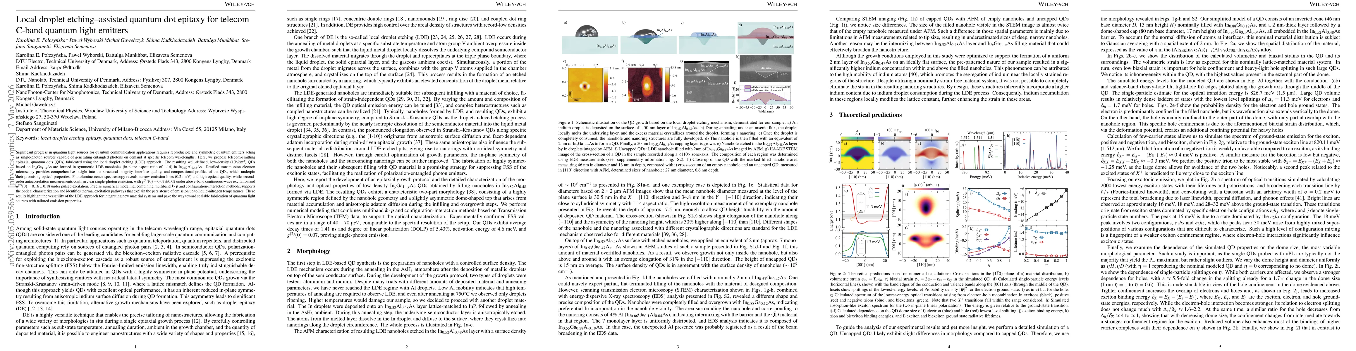
Significant progress in quantum light sources for quantum communication applications requires reproducible and symmetric quantum emitters acting as single-photon sources capable of generating entangled photons on demand at specific telecom wavelengths. Here, we propose telecom-emitting epitaxial quantum dots (QDs) fabricated using the local droplet etching (LDE) approach. The resulting well-defined, low-density ($10^9$/cm$^2$) QDs based on In$_{x}$Ga$_{1-x}$As are formed in symmetric LDE nanoholes (in-plane aspect ratio of 1.14) in In$_{0.52}$Al$_{0.48}$As. Detailed transmission electron microscopy provides comprehensive insight into the structural integrity, interface quality, and compositional profiles of the QDs, which underpin their promising optical properties. Photoluminescence spectroscopy reveals narrow emission lines (0.2 meV) and high optical quality, while second-order autocorrelation measurements confirm clear single-photon emission, with $g^{(2)}(0)=0.07\pm0.02$ under above-band continuous-wave excitation and $g^{(2)}(0)=0.16 \pm 0.18$ under pulsed excitation. Precise numerical modeling, combining multiband $\boldsymbol{k} \cdot \boldsymbol{p}$ and configuration-interaction methods, supports the optical characterization and identifies thermal excitation pathways that explain the persistence of emission up to liquid-nitrogen temperatures. These results highlight the versatility of the LDE approach for integrating new material systems and pave the way toward scalable fabrication of quantum light sources with tailored emission properties.
AI Key Findings
Generated May 08, 2026
Methodology — What approach did the authors take?
The study combines local droplet etching (LDE) to form symmetric nanoholes in In0.52Al0.48As, followed by infilling with InxGa1−xAs to create low-density QDs. Detailed TEM and AFM characterizations assess morphology, interfaces, and symmetry. Optical properties are evaluated via photoluminescence spectroscopy, second-order autocorrelation (g2(0)) under CW and pulsed excitation, and time-resolved PL. Numerical modeling uses multiband k·p and configuration-interaction methods to interpret emission and thermal activation pathways, supported by temperature-dependent measurements.
Key Results — What are the main findings?
- Low-density InxGa1−yAs QDs formed in symmetric LDE nanoholes with high in-plane symmetry and narrow emission lines (~0.2 meV).
- Single-photon emission is demonstrated with g2(0) = 0.07 ± 0.02 under above-band CW excitation and g2(0) = 0.16 ± 0.18 under pulsed excitation.
- FSS values are experimentally constrained to be below 70 μeV for several QDs, indicating potential for polarization-entangled emission.
- Average radiative decay time ~1.41 ns with a degree of linear polarization around 5–6%, indicating a high-quality optical confinement.
- TEM-based structural insight supports correlation between symmetry, interface quality, and observed optical performance.
Significance — Why does this research matter?
Demonstrates a scalable LDE-based route to telecom-band quantum dot emitters with low density and near-high in-plane symmetry, enabling low-FSS and potential on-demand entangled-photon emission suitable for quantum communication applications.
Technical Contribution — What is the technical contribution?
Introduces LDE-based epitaxy to create InxGa1−yAs QDs in symmetric nanoholes within In0.52Al0.48As, coupled with multiband k·p and configuration-interaction modeling to interpret optical properties and thermal activation mechanisms.
Novelty — What is new about this work?
Presents a telecom-band QD fabrication strategy that yields low-density, highly symmetric QDs via LDE with detailed TEM/AFM characterization and supports polarization-entangled emission prospects through ultra-low FSS and controlled optical dynamics.
Limitations — What are the limitations of this study?
- Exact FSS values are challenging to measure for very low-intensity lines, leaving some QDs with undetermined fine-structure characteristics.
- Emission persists up to 60 K but requires cryogenic temperatures for stable single-photon behavior, limiting practical deployment.
- Domain-specific optimization needed to fully suppress non-radiative channels and further increase emission stability at higher temperatures.
Future Work — What did the authors propose for future work?
- Refine filling-step to prevent dome accumulation and increase hole/electron level spacing by ~3×, aiming for higher thermal robustness.
- Systematically optimize QD size and symmetry to achieve consistently lower FSS across devices.
- Explore integration with photonic structures to enhance extraction efficiency and enable room-temperature operation pathways.
Paper Details
How to Cite This Paper
@article{munkhbat2026local,
title = {Local droplet etching-assisted quantum dot epitaxy for telecom C-band quantum light emitters},
author = {Munkhbat, Battulga and Semenova, Elizaveta and Połczyńska, Karolina E. and others},
year = {2026},
eprint = {2605.05956},
archivePrefix = {arXiv},
primaryClass = {physics.optics},
}
Munkhbat, B., Semenova, E., Połczyńska, K., Gawełczyk, M., Wyborski, P., Kadkhodazadeh, S., & Sanguinetti, S. (2026). Local droplet etching-assisted quantum dot epitaxy for telecom C-band quantum light emitters. arXiv. https://arxiv.org/abs/2605.05956
Munkhbat, Battulga, et al. "Local droplet etching-assisted quantum dot epitaxy for telecom C-band quantum light emitters." arXiv, 2026, arxiv.org/abs/2605.05956.
PDF Preview
Similar Papers
Found 4 papersCoherent light scattering from a telecom C-band quantum dot
L. Wells, T. Müller, R. M. Stevenson et al.
GaAs quantum dots grown by droplet etching epitaxy as quantum light sources
Saimon Filipe Covre da Silva, Gabriel Undeutsch, Barbara Lehner et al.
Spin properties in droplet epitaxy-grown telecom quantum dots
Marius Cizauskas, Elisa M. Sala, Jon Heffernan et al.
Optical spin tomography in a telecom C-band quantum dot
Junyang Huang, Ginny Shooter, Petros Laccotripes et al.
Comments (0)