Publication
Metrics
AI Quick Summary
This paper presents a local laser-induced solid-phase recrystallization method for optimizing phosphorus-implanted Si/SiGe heterostructures, achieving ohmic contacts without compromising layer precision, and demonstrates comparable or superior electron mobility and contact resistance at temperatures below 4.2 K. The method uses optical inspection for calibration and reduces thermal load on the active device area.
Paper Preview
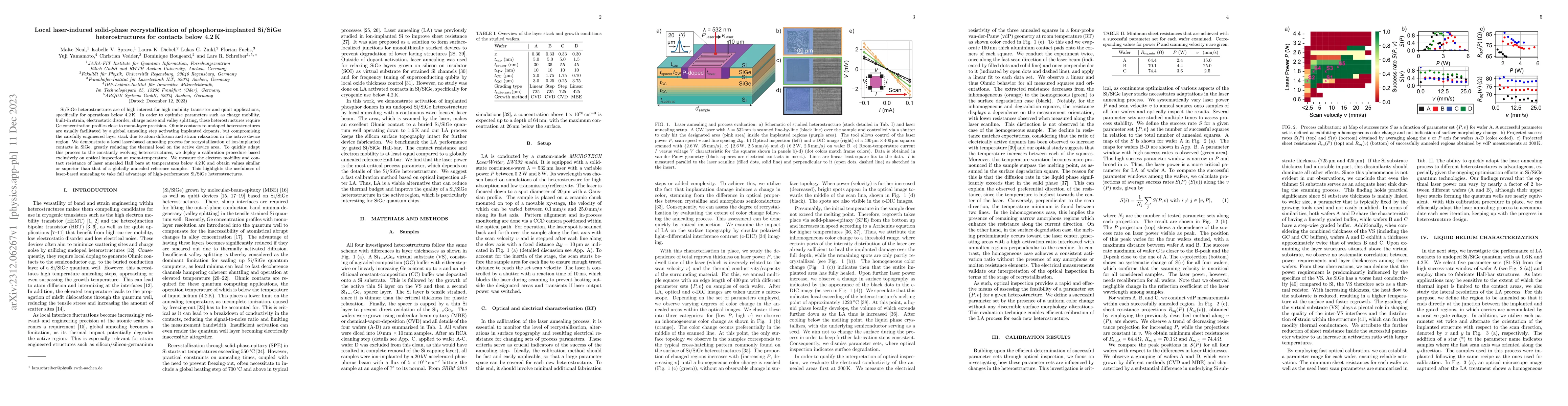
Abstract
Si/SiGe heterostructures are of high interest for high mobility transistor and qubit applications, specifically for operations below 4.2 K. In order to optimize parameters such as charge mobility, built-in strain, electrostatic disorder, charge noise and valley splitting, these heterostructures require Ge concentration profiles close to mono-layer precision. Ohmic contacts to undoped heterostructures are usually facilitated by a global annealing step activating implanted dopants, but compromising the carefully engineered layer stack due to atom diffusion and strain relaxation in the active device region. We demonstrate a local laser-based annealing process for recrystallization of ion-implanted contacts in SiGe, greatly reducing the thermal load on the active device area. To quickly adapt this process to the constantly evolving heterostructures, we deploy a calibration procedure based exclusively on optical inspection at room-temperature. We measure the electron mobility and contact resistance of laser annealed Hall bars at temperatures below 4.2 K and obtain values similar or superior than that of a globally annealed reference samples. This highlights the usefulness of laser-based annealing to take full advantage of high-performance Si/SiGe heterostructures.
AI Key Findings
Get AI-generated insights about this paper's methodology, results, significance, and more — seven facets brought into focus.
Impact
Paper Details
Authors
PDF Preview
Key Terms
Citation Network
Current paper (gray), citations (green), references (blue)
Display is limited for performance on very large graphs.
Discussion 0