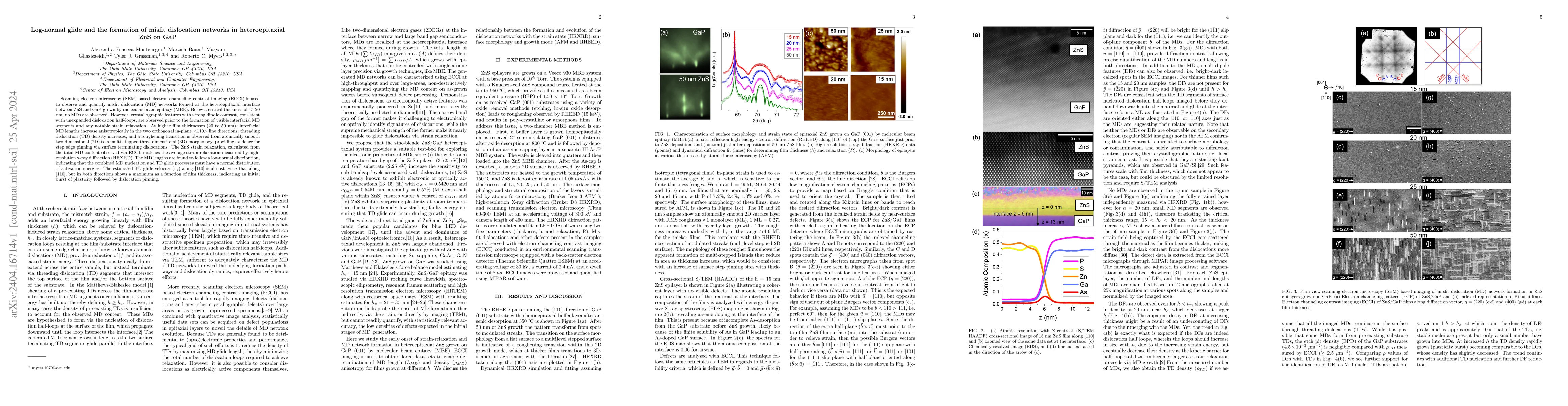
Kinetic Monte Carlo simulations for AlN and AlGaN epitaxial growth on AlN
|
W. Miller, T. Schulz, L. Lymperakis, A. Klump, M. Albrecht
|
2023
|
View Paper
|
Step pinning and hillock formation in (Al,Ga)N films on native AlN substrates
|
T. Schulz, S. Yoo, L. Lymperakis, C. Richter, E. Zatterin, A. Lachowski, C. Hartmann, H. Foronda, C. Brandl, H. Lugauer, M. Hoffmann, M. Albrecht
|
2022
|
View Paper
|
Harnessing dislocation motion using an electric field
|
Mingqiang Li, Yidi Shen, K. Luo, Qi An, Peng Gao, Penghao Xiao, Y. Zou
|
2022
|
View Paper
|
Dislocations as natural quantum wires in diamond
|
Sevim Polat Genlik, R. Myers, M. Ghazisaeidi
|
2022
|
View Paper
|
Correlation of early-stage growth process conditions with dislocation evolution in MOCVD-based GaP/Si heteroepitaxy
|
J. Boyer, Ari N. Blumer, Zak H. Blumer, Daniel L. Lepkowski, T. Grassman
|
2021
|
View Paper
|
Electron channeling contrast imaging investigation of stacking fault pyramids in GaP on Si nucleation layers
|
Markus Feifel, J. Ohlmann, R. France, D. Lackner, F. Dimroth
|
2020
|
View Paper
|
Quantitative Characterization of Misfit Dislocations at GaP/Si Heteroepitaxial Interfaces via Electron Channeling Contrast Imaging and Semi-Automated Image Analysis
|
Ari N. Blumer, J. Boyer, J. Deitz, Francisco A. Rodriguez, T. Grassman
|
2019
|
View Paper
|
Misfit-Dislocation Distributions in Heteroepitaxy: From Mesoscale Measurements to Individual Defects and Back
|
F. Rovaris, M. Zoellner, P. Zaumseil, M. Schubert, A. Marzegalli, L. Gaspare, M. Seta, T. Schroeder, P. Storck, G. Schwalb, C. Richter, T. Schülli, G. Capellini, F. Montalenti
|
2018
|
View Paper
|
Direct observation of recombination-enhanced dislocation glide in heteroepitaxial GaAs on silicon
|
P. Callahan, Brian B. Haidet, Da-Hoon Jung, G. Seward, K. Mukherjee
|
2018
|
View Paper
|
Extraordinary plasticity of an inorganic semiconductor in darkness
|
Y. Oshima, A. Nakamura, K. Matsunaga
|
2018
|
View Paper
|
Calculated electronic, transport, and bulk properties of zinc-blende zinc sulphide (zb-ZnS)
|
Bethuel Khamala, Lashounda Franklin, Y. Malozovsky, A. Stewart, H. Saleem, D. Bagayoko
|
2016
|
View Paper
|
Nobel Lecture: Background story of the invention of efficient blue InGaN light emitting diodes
|
S. Nakamura
|
2015
|
View Paper
|
Applications of Electron Channeling Contrast Imaging for the Rapid Characterization of Extended Defects in III–V/Si Heterostructures
|
S. Carnevale, J. Deitz, J. Carlin, Y. Picard, D. McComb, M. De Graef, S. Ringel, T. Grassman
|
2015
|
View Paper
|
Strain release management in SiGe/Si films by substrate patterning
|
V. Mondiali, M. Bollani, D. Chrastina, R. Rubert, G. Chahine, M. Richard, S. Cecchi, L. Gagliano, E. Bonera, T. Schülli, L. Miglio
|
2014
|
View Paper
|
Theory of dynamical electron channeling contrast images of near-surface crystal defects.
|
Y. Picard, M. Liu, Joel Lammatao, R. Kamaladasa, M. Graef
|
2014
|
View Paper
|
Rapid misfit dislocation characterization in heteroepitaxial III-V/Si thin films by electron channeling contrast imaging
|
S. Carnevale, J. Deitz, J. Carlin, Y. Picard, M. Graef, S. Ringel, T. Grassman
|
2014
|
View Paper
|
Surface morphology of homoepitaxial c-plane GaN: Hillocks and ridges
|
F. Oehler, T. Zhu, S. Rhode, M. Kappers, C. Humphreys, R. Oliver
|
2013
|
View Paper
|
Recipes for the fabrication of strictly ordered Ge islands on pit-patterned Si(001) substrates
|
M. Grydlik, G. Langer, T. Fromherz, F. Schäffler, M. Brehm
|
2013
|
View Paper
|
Lattice relaxation of ZnS grown on GaP investigated by high‐resolution X‐ray diffraction and transmission electron microscopy
|
K. Ichino, Akinori Nishigaki, Akiyoshi Yamauchi
|
2012
|
View Paper
|
Effect of misfit dislocation on surface diffusion
|
M. Aminpour, O. Trushin, T. Rahman
|
2010
|
View Paper
|
Dislocations as Active Components in Novel Silicon Devices
|
M. Kittler, M. Reiche
|
2009
|
View Paper
|
Nondestructive analysis of threading dislocations in GaN by electron channeling contrast imaging
|
Y. Picard, J. Caldwell, M. Twigg, C. Eddy, M. Mastro, R. Henry, R. Holm, P. Neudeck, A. J. Trunek, J. Powell
|
2007
|
View Paper
|
Scanning electron microscopy imaging of dislocations in bulk materials, using electron channeling contrast
|
M. Crimp
|
2006
|
View Paper
|
Thin Film Materials: Stress, Defect Formation and Surface Evolution
|
L. Freund, S. Suresh
|
2004
|
View Paper
|
Resonant Raman scattering measurements of strains in ZnS epilayers grown on GaP
|
Y. Yu, M. Hyun, Sungun Nam, Donghan Lee, O. Byungsung, Kwang-Cheol Lee, P. Yu, Y. Choi
|
2002
|
View Paper
|
Growth of (Zn,Cd)S and (Zn,Mg)S containing structures on GaP
|
K. Prior, S. Telfer, Xiaodong Tang, C. Morhain, B. Urbaszek, C. O'Donnell, P. Tomasini, A. Balocchi, B. Cavenett
|
2001
|
View Paper
|
Dislocation mediated surface morphology of GaN
|
B. Heying, E. Tarsa, C. Elsass, P. Fini, S. Denbaars, J. Speck
|
1999
|
View Paper
|
Interfaces
|
M. Olsson
|
1998
|
View Paper
|
Solid phase recrystallization of ZnS thin films on sapphire
|
Z. Bandic, E. Piquette, J. McCaldin, T. C. Mcgill
|
1998
|
View Paper
|
Lattice relaxation in ZnS epilayers grown on GaP
|
Sungun Nam, Jongkwang Rhee, Y. Yu, Chong-kook Lee, O. Byungsung, K. Lee, Y. Choi
|
1998
|
View Paper
|
Growth and characterization of light emitting ZnS/GaN heterostructures
|
E. Piquette, Z. Bandic, J. McCaldin, T. C. Mcgill
|
1997
|
View Paper
|
Formation of stacking faults in ZnS thin films epitaxially grown on GaAs(001)
|
M. Arnold, Zhong Lin Wang, W. Tong, B. Wagner, S. Schön, C. Summers
|
1997
|
View Paper
|
Anisotropic strain relaxation of GaInP epitaxial layers in compression and tension
|
M. Matragrano, D. Ast, J. Shealy, V. Krishnamoorthy
|
1996
|
View Paper
|
Ultra High Vacuum Reflection Electron Microscopy Study of Step-Dislocation Interaction on Si(111) Surface
|
A. Latyshev, H. Minoda, Y. Tanishiro, K. Yagi
|
1995
|
View Paper
|
Correlation of anisotropic strain relaxation with substrate misorientation direction at InGaAs/GaAs(001) interfaces
|
R. Goldman, H. Wieder, K. Kavanagh
|
1995
|
View Paper
|
Molecular‐beam epitaxy of ZnS using an elemental S source
|
J. Cook, D. Eason, R. Vaudo, J. Schetzina
|
1992
|
View Paper
|
Valence band offset in ZnS layers on Si(111) grown by molecular beam epitaxy
|
C. Maierhofer, S. Kulkarni, M. Alonso, T. Reich, K. Horn
|
1991
|
View Paper
|
Anisotropic defect distribution in ZnSe/ZnS epitaxial layers grown by metalorganic vapor‐phase epitaxy on (001)‐oriented GaAs
|
P. Brown, G. Russell, J. Woods
|
1989
|
View Paper
|
Low resistivity Al-doped ZnS grown by MOVPE
|
T. Yasuda, K. Hara, H. Kukimoto
|
1986
|
View Paper
|
Stacking-fault energy of II–VI compounds
|
S. Takeuchi, Kunio Suzuki, K. Maeda, H. Iwanaga
|
1985
|
View Paper
|
Defects in epitaxial multilayers: I. Misfit dislocations*
|
J. W. Matthews, A. Blakeslee
|
1974
|
View Paper
|
Misfit strain and misfit dislocations in lattice mismatched epitaxial layers and other systems
|
S. Jain, A. Harker, R. Cowley
|
1997
|
View Paper
|
Transmission Electron Microscopy: A Textbook for Materials Science
|
David B. Williams, C. B. Carter
|
1996
|
View Paper
|
Behaviour of dislocations in GaAs revealed by etch pit technique and X-ray topography
|
I. Yonenaga, K. Sumino
|
1993
|
View Paper
|
Misfit dislocations in lattice-mismatched epitaxial films
|
R. Hull, J. Bean
|
1992
|
View Paper
|
The photoplastic effect in wurtzite and sphalerite structure II–VI compounds
|
C. Ahlquist, M. Carroll, P. Stroempl
|
1972
|
View Paper
|
Comments (0)